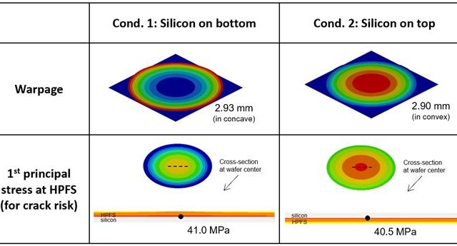
Challenges and associated solutions in using glass in a standard 300mm Si fab are discussed. We demonstrate that functionalized glass wafers can pass all the requirements to enter a Si fab to enable layer transfer of RF components.
Wooptix Introduces Wafer Geometry System for 300mm Blank Silicon Wafers
Wooptix SL, a Spanish company dedicated to developing new imaging solutions, has introduced Phemet® lab system, a 300mm blank silicon wafer geometry system collecting millions of topography data points on a full wafer in a few seconds.
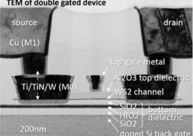
A 300mm Platform for 2D-Material Based MOSFET Devices
2D materials, a family of materials that form two-dimensional crystals, promise to enable a broad range of semiconductor applications, such as selectors or back-end compatible transistors.
XMC becomes YRST or Changjiang Storage
As reported by Digitimes, a major enterprise in Wuhan, China has broken ground on the first of three mega-fabs to produce 3D-NAND chips. The final fab name-plate may ultimately read XMC or YMTC or YRST or possibly Changjiang Storage (not…
China to be 15% of World Fab Capacity by 2018
Currently there are eight Chinese 300mm-diameter silicon IC fabs in operation as 2016 comes to a close. Chinese IC fab capacity now accounts for approximately 7% of worldwide 300mm capacity, as reported by VLSIresearch in a recent edition of its…
Leti Shows MEMS on 300mm Wafers
As reported by EETimes from the European MEMS Summit last month, French research institute CEA-Leti has manufactured accelerometer MEMS devices on 300mm-diameter wafers. This technology is currently being transferred to Tronics Microsystems SA (Grenoble, France), which currently only manufactures on…
300mm ams Fab Bet on IoT
Leading-edge IC fab investments are multi-billion-dollar risky bets. Insufficient demand for ICs dooms the line to economic failure regardless of the quality of design and manufacturing. Thus, it is a big deal that Austrian-headquartered ams AG—world leader in production of…
No technical barriers seen for 450mm
Paul Farrar, general manager of the G450C consortium, said early work has demonstrated good results and that he sees no real barriers to implementing 450mm wafers from a technical standpoint.