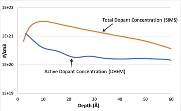
Electrical property depth profile data from semiconductor films can be obtained using the Differential Hall Effect Metrology approach. The technique can yield sub-nm depth resolution for Si and Ge. For III-V compounds depth resolution is ~1 nm.
Electrical property depth profile data from semiconductor films can be obtained using the Differential Hall Effect Metrology approach. The technique can yield sub-nm depth resolution for Si and Ge. For III-V compounds depth resolution is ~1 nm.
| Cookie | Duration | Description |
|---|---|---|
| cookielawinfo-checkbox-advertisement | 1 year | The cookie is set by GDPR cookie consent to record the user consent for the cookies in the category "Advertisement". |
| cookielawinfo-checkbox-analytics | 11 months | This cookie is set by GDPR Cookie Consent plugin. The cookie is used to store the user consent for the cookies in the category "Analytics". |
| cookielawinfo-checkbox-functional | 11 months | The cookie is set by GDPR cookie consent to record the user consent for the cookies in the category "Functional". |
| cookielawinfo-checkbox-necessary | 11 months | This cookie is set by GDPR Cookie Consent plugin. The cookies is used to store the user consent for the cookies in the category "Necessary". |
| cookielawinfo-checkbox-others | 11 months | This cookie is set by GDPR Cookie Consent plugin. The cookie is used to store the user consent for the cookies in the category "Other. |
| cookielawinfo-checkbox-performance | 11 months | This cookie is set by GDPR Cookie Consent plugin. The cookie is used to store the user consent for the cookies in the category "Performance". |
| viewed_cookie_policy | 11 months | The cookie is set by the GDPR Cookie Consent plugin and is used to store whether or not user has consented to the use of cookies. It does not store any personal data. |
| Cookie | Duration | Description |
|---|---|---|
| _ga | 2 years | This cookie is installed by Google Analytics. The cookie is used to calculate visitor, session, campaign data and keep track of site usage for the site's analytics report. The cookies store information anonymously and assign a randomly generated number to identify unique visitors. |
| _gat_gtag_UA_142332005_1 | 1 minute | This cookie is set by Google and is used to distinguish users. |
| _gid | 1 day | This cookie is installed by Google Analytics. The cookie is used to store information of how visitors use a website and helps in creating an analytics report of how the website is doing. The data collected including the number visitors, the source where they have come from, and the pages visted in an anonymous form. |
| _pk_id.56353.85f6 | 1 year 27 days | This cookie is set by Google Analytics and is used to store a unique user ID for statistical purposes. |
| _pk_ses.56353.85f6 | 30 minutes | This cookie is created by Piwik PRO to store a unique session ID. |
| CONSENT | 16 years 5 months 18 days 3 hours | These cookies are set via embedded youtube-videos. They register anonymous statistical data on for example how many times the video is displayed and what settings are used for playback.No sensitive data is collected unless you log in to your google account, in that case your choices are linked with your account, for example if you click “like” on a video. |
| Cookie | Duration | Description |
|---|---|---|
| IDE | 1 year 24 days | Used by Google DoubleClick (which we don't use) and stores information about how the user uses the website and any other advertisement before visiting the website. This is used to present users with ads that are relevant to them according to the user profile. |
| test_cookie | 15 minutes | This cookie is set by doubleclick.net. The purpose of the cookie is to determine if the user's browser supports cookies. |
| VISITOR_INFO1_LIVE | 5 months 27 days | This cookie is set by Youtube. Used to track the information of the embedded YouTube videos on a website. |
| YSC | session | This cookies is set by Youtube and is used to track the views of embedded videos. |
| Cookie | Duration | Description |
|---|---|---|
| optin | 1 hour | This cookie tracks users who take an affirmative action, such as checking a tick-box or another similar action. The consent is used for a variety of purposes, such as agreeing to terms and conditions, signing up for online content like newsletters and resources, consenting to the use of cookies, and more. |
| yt-remote-connected-devices | never | Stores the user's video player preferences using embedded YouTube video. |
| yt-remote-device-id | never | Stores the user's video player preferences using embedded YouTube video. |