Nordson Test & Inspection will unveil the new Quadra 7 Pro Manual X-Ray Inspection (MXI) system at SEMICON China.

New Wafer-like and Reticle-like Sensors Deliver Fast, Easy Measurements Inside the Process Chamber
Sensors are available for a range of routine and specialized applications. The two newest sensors offer significant advancements in terms of performance and range of application.
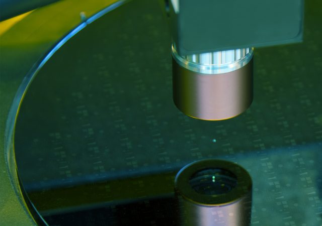
An Interview with Kistler’s Robert Hillinger
Robert Hillinger, Business Development Manager at Kistler, explains how dynamic force measurement increases process reliability in semiconductor production.
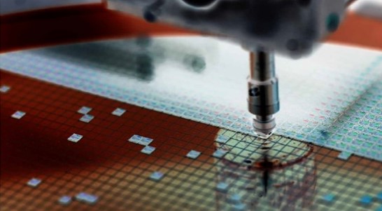
Emerging Metrology Requirements for Heterogeneous Integration and 3D Packaging
The ability to speed up the deployment of heterogeneous integration in mass production requires new and more frequent types of measurements in key manufacturing processes, including wafer and die bonding as well as lithography.
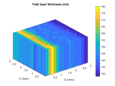
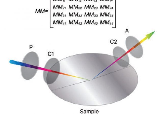
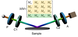
Multilayer Thickness Evaluation of Semiconductor and Display Structures by Picosecond Ultrasonics
The product line JAX designed by Neta uses unique properties of femtosecond pulses and photo-acoustic effects to inspect thin films stacks. This 100% non-destructive optical method can be used to test and control multilayers which are typical from applications in the semiconductor or in the display industries.
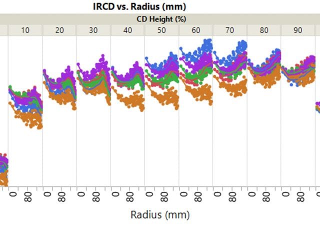
Mid-Infrared Optical Metrology for High Aspect Ratio Holes in 3D NAND Manufacturing
Infrared critical dimension metrology (IRCD) addresses the shortcomings of conventional ultraviolet to near-infrared OCD in channel hole etch high-fidelity z-profile and amorphous carbon hardmask etch BCD metrology.
Metrology Solutions for Gate-All-Around Transistors in High Volume Manufacturing
High-speed, non-destructive OCD metrology has the capability needed to support process control throughout the GAA process flow.
Onto Innovation: A Mid-Year Update
Onto Innovation (ONTO), created last year by a merger of Rudolph and Nanometrics, focuses primarily on optical metrology, macro defect inspection, process control software, and panel lithography.
Artificial Intelligence and Machine Learning in Semiconductor Manufacturing: Inspection and Metrology
AI and ML have great potential in many areas of the semiconductor manufacturing process, ranging in scale from improving the performance of individual tools to managing an entire fab and optimizing the global supply chain
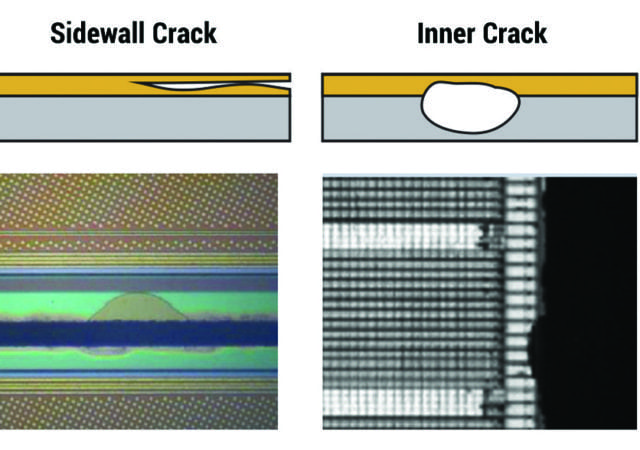
Die Crack Detection in HVM is Critical for High Reliability Applications
The detection of cracks after the wafer is diced into individual die has become critical in high reliability applications, like the automotive market, where there are substantial safety and liability concerns.