A new report predicts that the global semiconductor packaging market will reach $60.44 billion by 2030 from $27.10 billion in 2020, growing at a CAGR of 9.10% from 2021 to 2030.
New Plating Tool for WLP and Plating in Compound Semi Manufacturing
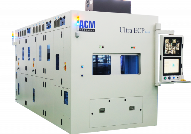
ACM’s Ultra ECP GIII plating tool is designed for WLP for compound semiconductors, with product offerings for SiC, GaN and GaAs. The tool is also capable of plating gold into backside deep hole processes with greater uniformity and better step coverage.
Apple Fab Speculation
Apple Corp. recent purchased an old 200mm-diameter silicon wafer fab in San Jose capable of creating as small as 90nm device features. Formerly owned and operated by Maxim, the US$18.2M purchase reportedly includes nearly 200 working fab tools. Some people…