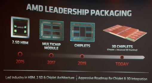
At Computex a couple of months ago Lisa Su of AMD gave a keynote talk detailing their new products, but at the tail end she surprised attendees by discussing their advancements in packaging technology. “We’ve worked closely over the last few years with TSMC on their 3D Fabric technology to combine chiplet packaging with die stacking to create a 3D chiplet architecture for future high-performance computing products.”

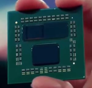
“The first application of this technology will be to enable a 3d vertical cache. In this prototype we’re taking our leadership Ryzen 5000 processor and stacking a 64 MB 7-nm SRAM directly on top of each core complex die, effectively tripling the L3 cache feeding our Zen 3 cores.” And there was a sample to show off:
Here the lid was removed from the package, exposing the left die stack so that we can see one of the 6 x 6 mm square SRAMs hybrid bonded to the core complex die (CCD) below.

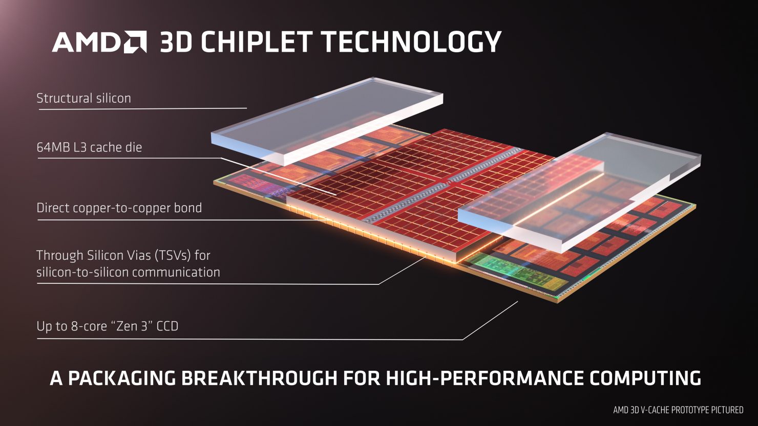
The SRAM die has been designed to sit on top of the L3 cache of the processor, connecting by both hybrid bonding and TSVs (through-silicon vias), and dummy silicon is added to provide strength and give a uniform top surface to the assembly.

AMD also uploaded a video showing the TSVs in more detail, here’s a screenshot:

There seems to be a bit of artistic license taken here – the top SRAM die is shown face up, but if hybrid bonding is used, it must be face down. It looks like the CCD has been flipped so that it can face-to-face (F2F) hybrid bond with the SRAM, so the TSVs connect the package substrate to the power and signal rails at the top of the die.
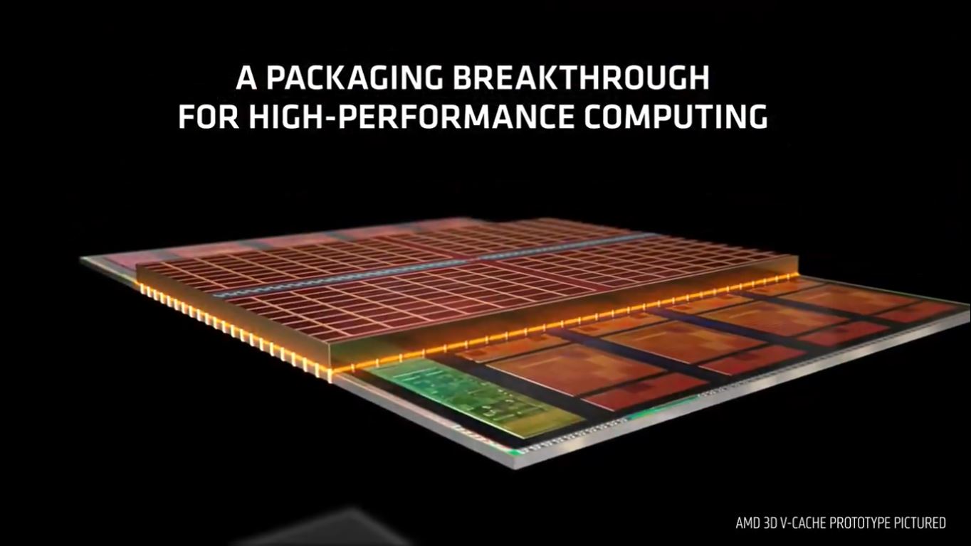
The final 3D product looks the same as current Ryzen 5000s, so presumably there is a redistribution layer (RDL) on the base of the CCD to link the TSVs to a bump pattern to match the existing bump pattern in the package. Both the CCD and the SRAM are thinned so that their total height matches that of the I/O chip and the same lid and heat-spreader can be used.
It is possible that the CCD is face down as normal (i.e., not as shown above), with the TSVs going through to the back surface of the die, and the SRAM die face-to-back (F2B) with an RDL on the back of the CCD die. That would save hassle with the CCD flip-chip bonding, but add some series resistance to the V-cache links, slowing it down, and also slow thermal dissipation from the active cores since there is more silicon in the way.

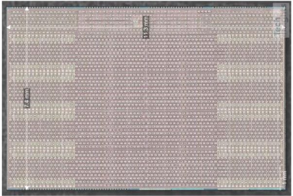
The Ryzen 5950 has 32 MB of L3 cache SRAM, organized into eight 4-MB blocks:
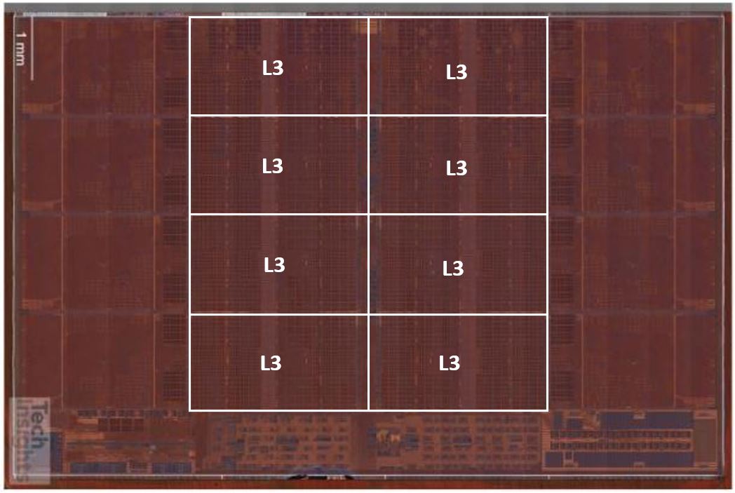

Each block is 2.86 x 1.55 mm, for a total block area of 35.5 mm2, so a 6 x 6 mm stack die is a good match to sit on the L3 cache of the CC die. Since there is no overlap over the cores, the heat dissipation from them is through the structural silicon above.
The stack SRAM is twice the density, fitting 64 MB into 36 mm2; AMD explained that it uses optimised SRAM libraries, and the existing CCD already has all control and power logic designed in. If the base die is already laid out for TSV usage, presumably it is not as tightly packed, since space will be needed for the TSVs and their keep-out zones, and block density will be lower than a non-TSV design.
TechInsights took another look at their existing Ryzen 5950X and did indeed find TSV sites on the SRAM area. Close examination showed a series of white dots in optical images of the L3 blocks:
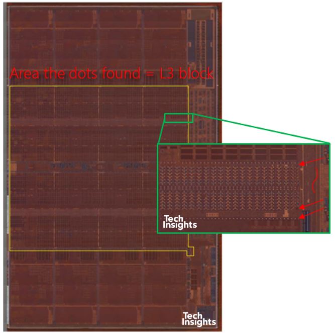

And a follow-up examination in the SEM showed that the white dots were TSV sites. The image below is at the gate level, and from a bevel-polished sample, which is why it fades out in the left half. The area inside the dummy features is ~2.7µm square, so one could guess that the TSV diameter is ~2.5 µm.
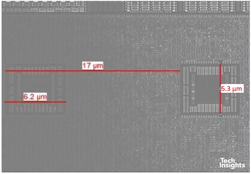

The die has 15 metal levels, including M0, and by continuing up the bevel TechInsights established that the TSVs connected at the M10 – M11 level, making it a via-middle technology.
By measuring the row lengths and number of rows, with the 17 µm pitch, they estimated the number of TSVs at ~23,000.
Not long after Computex, this tweet appeared from Nemez, who clearly had access to a high-resolution die photo of the 5950X, and did a detailed count, coming up with a total of 24,070:
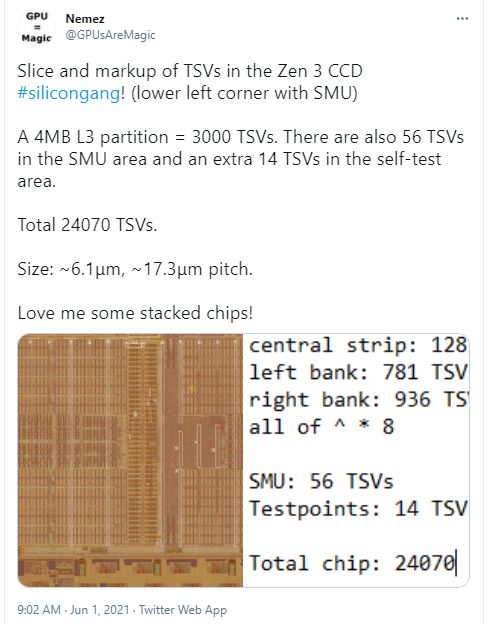

The TSV size and pitch estimates are surprisingly accurate! Expanding his photo, we see the locations of the TSVs.

Some basic math shows us that 24,000 TSV keep-out zones is ~0.8 mm2, so there are other factors affecting the SRAM density in the CCD. If we take the TSV diameter to be ~2.5 µm, then with guesstimated aspect ratios of 10:1 – 20:1, we get an estimated die thickness of 25 – 50 µm.
The die mark on the 5950X has a design date of 2019, so clearly AMD was contemplating stacked SRAM integration a while ago; TSMC’s TSV capability is well established from its years of interposer experience, and AMD could have gone with micro-bump stacking, but chose to wait until hybrid bonding was production ready.
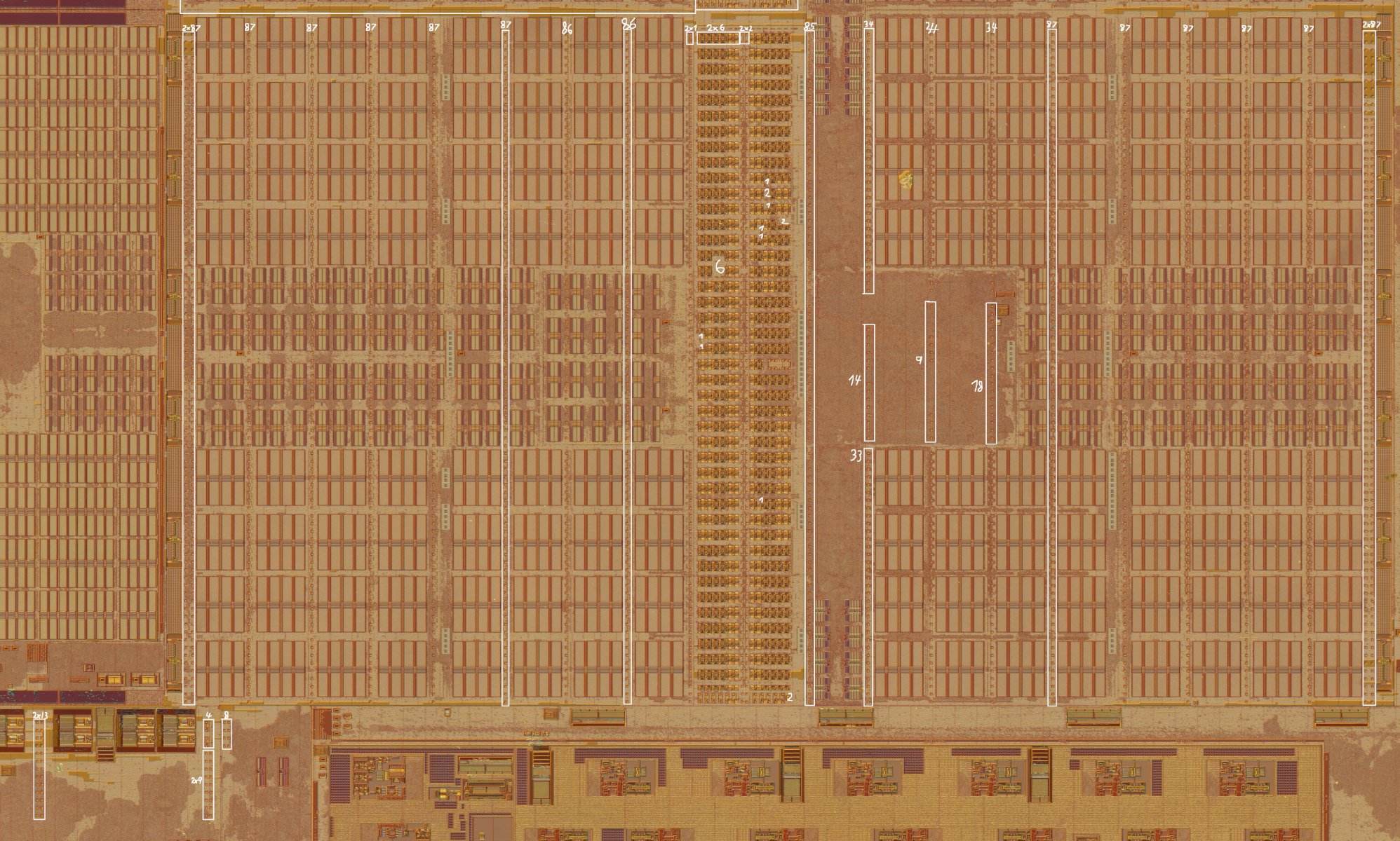
TSMC has had their CoWoS TSV technology for almost ten years now; this is an example of a TSV from a Xilinx Virtex-7 interposer die:

We can see that the TSV connects with M1 of the interposer, and we have a ~10:1 aspect ratio.
The Ryzen 5000 series has two CCDs plus the I/O die in the package, for a total of 64 MB SRAM per device. With the V-cache adding an additional 128 MB, we have a total of 192 MB in the upgraded part, with the bandwidth of the L3 cache claimed to increase to over 2 TB/sec. The first products go into production at the end of the year.
At the moment only a single SRAM die stack is planned, but the TSV/F2F technology makes higher stacks possible. The comment was made that SRAM is usually less exercised than the cores, so thermal dissipation is less of an issue, and the die(s) will also be thinned down, reducing thermal resistance; and the TSVs going up through a multi-die stack will also help heat dispersal.
Coincidentally, TSMC held their Technology Symposia the same week as Computex, and one of the announcements was that their chip-on-wafer (CoW) version of SoIC™ (System on Integrated Chips) will be qualified for N7-on-N7 this year, with production slated for next year. Given that both the CCD and the V-cache are 7-nm, the new Ryzen 5000 sounds like the first product to use this technology.
The SoIC technology was introduced at ECTC 2019 [1], including stacking with TSVs, and TSMC showed an example at last year’s Technology Symposium:

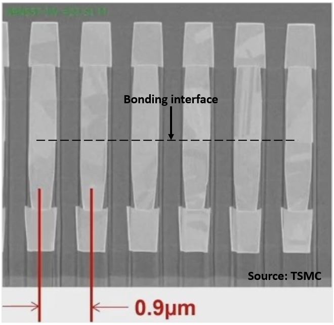

And they have pushed the pitch down to less than a micron:
We’ll be looking for the new Ryzen 5950 – will it be F2F or F2B?
Reference
- C. Chen, et al., “System on Integrated Chips (SoICTM) for 3D Heterogeneous Integration”, ECTC 2019, pp. 594 – 599