By Dick James
Less than two weeks after IBM announced their 2-nanometer CMOS technology, UK website Verdict picked up on a paper published in Nature and somehow morphed that into a claim that TSMC had made breakthrough in 1-nm technology development, and that was subsequently circulated by much of the tech press that I follow (search “TSMC & 1nm”!).
The Verdict headline was “TSMC trumps IBM’s “2nm” chip tech hyperbole with “1nm” claim”, referring to a Nature publication “Ultralow contact resistance between semimetal and monolayer semiconductors”[1].
The essence of the paper is the use of bismuth (Bi) to provide contact to a molybdenum disulphide (MoS2) monolayer transistor, achieving a claimed record low contact resistance of 123 Ω µm, and a record high on-state current density of 1,135 µA/µm.
The authors state that “This technology unveils the potential of high-performance monolayer transistors that are on par with state-of-the-art three-dimensional semiconductors, enabling further device downscaling and extending Moore’s law.” No mention that I could see of a specific 1 nm technology.
The paper was a joint presentation from MIT, TSMC, UC Berkeley, National Taiwan University (NTU), and the King Abdullah University of Science & Technology (KAUST) in Saudi Arabia, with 23 authors in all. It was submitted on 1 July last year, and published 12 May.
There does not appear to be any information on the paper on either the TSMC or NTU websites, but a press release from MIT explains that one of the challenges in the use of monolayers is the contact resistance between the metal contact electrode and the monolayer, and using a semi-metal such as bismuth reduces or eliminates the Schottky barrier at the contact interface.
It further goes on to say that 2D monolayers “meet all the requirements for enabling a further leap in miniaturization of transistors, potentially reducing by several times a key parameter called the channel length — from around 5 to 10 nanometers, in current cutting-edge chips, to a subnanometer scale.”
Aside from the confusion between technology node and channel length (not unusual in the technical press), the sub-nm scale comment is the only reference I can find to a process generation.
That said, TSMC has been collaborating with MIT, NTU and quite a lot of other organisations for a while, and this is not the first time we have seen MoS2 as a topic from them. At last year’s VLSI Symposium authors from the same group presented on monolayer MoS2 devices [2], and at the 2020 IEDM a collaboration with National Chiao Tung University looked at edge contacts to MoS2 FETs [3].
Ultralow Contact Resistance
A conventional metal contact has a Schottky barrier at the interface which gives high contact resistance. In current technology, we try and reduce the barrier by heavily doping the semiconductor, and/or putting a thin dielectric layer at the interface; but it’s hard to highly dope a monolayer, and an extra dielectric layer adds a tunnelling barrier. The state-of-the-art contact resistance reported in [2] was ~1.1 kΩ-μm, at least one order of magnitude larger than metal–Si contacts.
A metal such as nickel induces gap states at the interface, creating energy barriers and giving high contact resistance; but bismuth is a semi-metal, and it suppresses the gap states and spontaneously forms degenerate states in the monolayer, giving zero Schottky barrier height.
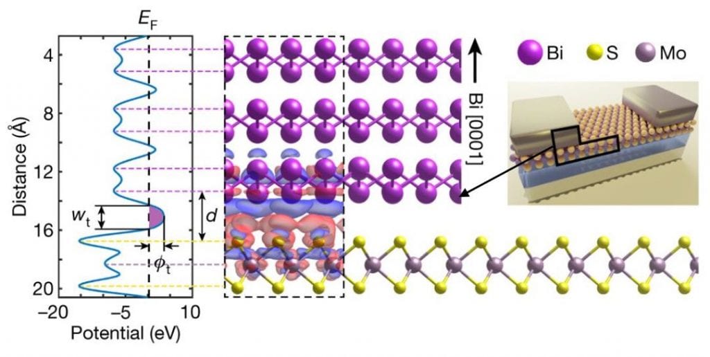
Below (Fig. 1) is a schematic of a Bi-MoS2 FET in the upper right, with the area outlined enlarged to its left and below, showing an atomic rendering; left of that is the corresponding electrostatic potential profile along the vertical direction, with the electron tunnelling barrier shaded in purple (width, wt = 0.166 nm; height, Φt = 3.6 eV). The distance between the Bi and S atomic layers d = 0.34 nm. The coloured regions at the interface within the dashed line in the atomic structure indicate the differential charge density (red = +ve, blue = -ve), calculated by subtracting the pre-contact charge density from the post-contact charge density.

The devices were fabricated by transferring the MOCVD or CVD MoS2 monolayers from growth substrates onto silicon nitride or silicon dioxide dielectric layers on P++ Si substrates, and 20 nm bismuth was e-beam deposited and given a gold capping layer. E-beam lithography was used to define the channel and source/drain contacts, with channel lengths of ~30 – 500 nm and channel widths of 2 – 10 μm. The P++ substrate was used as a back-gate for transistor operation.
The effect of the reduced barrier can be seen in Fig. 2(a) – by plotting total device resistance vs channel length for different carrier densities (N2D), the intercept on the vertical axis (zero channel length) will be twice the contact resistance RC, giving a RC value of ~123 Ω-μm. The inset SEM image is a false colour image of the test structure.
In Fig. 2(b) the difference between nickel and bismuth contacts is clear; the IDS – VDS characteristic of a Bi-MoS2 FET (VGS = 60V) at low temperature is linear and Ohmic, and the Ni-MoS2 FET shows the effect of the Schottky barrier.

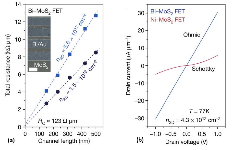
Fig. 3 below shows IDS – VDS curves of Bi–MoS2 FETs with channel lengths of 120 and 35 nm on 100-nm-thick SiNxgate dielectrics. The linear relationships at low-field indicate ohmic contacts, leading to high ION/IOFF current ratios (>107) and very high drive current for monolayer transistors with a drain voltage of 1.5 V. The inset is a SEM image of the 35-nm device.

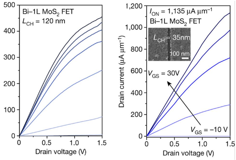
The highest values of ION achieved were 560 μA/μm for the 120-nm LCH, and 1,135 μA/μm for the 35-nm LCH devices. That compares with a highest nFET current of 390 μA/μm at VDS = 1 V for a 100-nm channel in [2], although that used 10 nm HfO2 as a gate dielectric layer.
As we noted earlier, the Bi contact resistance was 123 Ω µm, and that reported in [2] was ~1.1 kΩ-μm, almost an order of magnitude better.
As a final comment, I have to say that the 1-nm claim looks like more journalistic hyperbole to me – nowhere in these works can I find any mention of a 1-nm process. Finding a good low-resistance contact to a 2D monolayer is a great step forward, but we are a long way from real product, so using a node number is pure imagination.
However, it did get a lot of press attention! South China Morning Post puts the technology at least ten years out…
References
- Shen, PC., et al., “Ultralow contact resistance between semimetal and monolayer semiconductors” Nature 593, 211–217 (2021).
- A-S Chou et al., “High On-Current 2D nFET of 390 µA/µm at V = 1V using Monolayer CVD MoS2 without Intentional Doping”, VLSI 2020, paper TN1.7
- Y.T Hung et al., “Pinning-Free Edge Contact Monolayer MoS2 FET”, IEDM 2020, paper 3.3, pp. 39 – 42