The advanced packaging market to grow at a CAGR of 8% to reach $55 billion by 2028 from ~$30 billion in 2020. The advanced packaging market growth is driven by the innovations in packaging technology, miniaturization of devices, and increasing adoption of MEMS. The advanced packaging technology to hold more than 60% share in semiconductor packaging market by 2030.
The Insight Partners added latest research study titled as, “Advanced Packaging Market Size, Share, Revenue, Growth, Global Analysis and Forecast to 2028”. According to the report, the Advanced Packaging Technologies to Contribute Significantly to Economic Recovery of Semiconductor Industry. Foundries, substrate/PCB suppliers, and EMS/DM Players, etc., operating with different business models entering packaging business.
Innovations in packaging technologies, and focus on heterogeneous integrations and wafer-level packages have prompted the chip industry to develop a new set of solutions, collectively known as advanced packaging. An increase in the size of silicon from 100 mm to 300 mm is a significant trend affecting the advanced packaging market. The shift to wafers with longer diameters has reduced the manufacturing cost by 20–25%. The miniaturization of devices and increasing adoption of MEMS are bolstering the demand for embedded die packaging. Though the technology is not new in the market, the adoption has been limited to niche applications due to high cost and low yield; however, it has immense potential for development in the future. Advancements in the Bluetooth and radiofrequency (RF) modules and the rise of Wi-Fi 6 could further fuel the advanced packaging industry. The continuous evolution of smartphones and tablets technologies, wireless communications, etc., will positively impact the progress of this industry.
Intel and Samsung (IDMs); TSMC (a foundry); ASE, SPIL, Amkor, PTI, and JCET (the Top 5 global OSATs); Nepes; and Chipbond are the 10 players that account for ~75% of global advanced packaging industry. The advanced packaging market is significantly driven by end user revenue because of the elevated demand for the latest technologies and high-speed gadgets. The companies have gained sustainable competitive advantages through innovations in this market, owing to the growing need for differentiated products for various applications.
- February 2021: Siemens Digital Industries Software announced a collaboration with Advanced Semiconductor Engineering, Inc. (ASE) to evaluate multiple complex integrated circuit (IC) package assemblies and interconnects in a data-robust graphical environment before and during physical design implementation.
- August 2020: Samsung Electronics announced the availability of its silicon-proven 3D IC packaging technology—eXtended-Cube (X-Cube)—for most advanced process nodes.
- May 2020: Synapse Electronique, a Canadian equipment electronics manufacturer and EMS provider, integrated two Universal Instruments Fuzion Platform production lines in its Shawinigan, Quebec facility.
There has been a paradigm shift in the packaging/assembly business in recent times. Although Outsourced Semiconductor Assembly and Tests (OSATs) and Integrated Device Manufacturers (IDMs) have been the key contributors to the market for a long, players with different business models—including foundries, substrate/Printed Circuit Board (PCB) suppliers, and Electronic Manufacturing Service (EMS) companies—are entering into the assembly/packaging business.
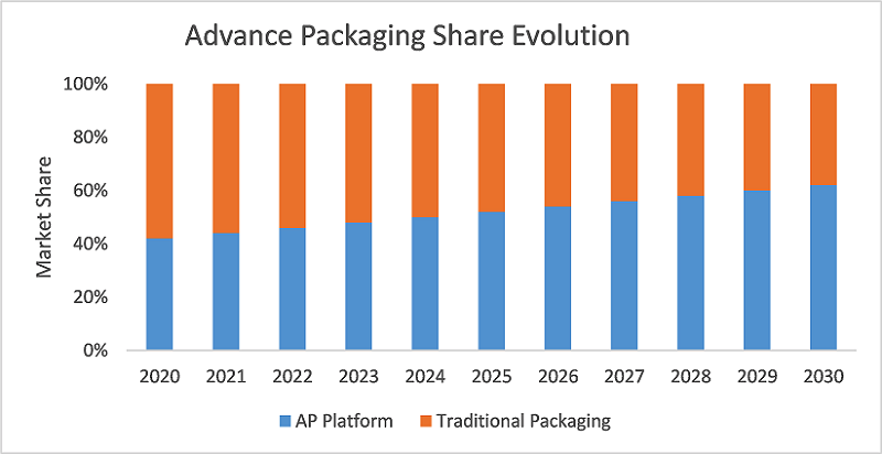
The advanced packaging industry held ~40% share in the semiconductor packaging market in 2020, and currently, the market is dominated by traditional packaging platforms. However, advanced packaging technologies are expected to account for more than 60% of the semiconductor packaging market by 2030.

The back-end process of supply chains requires significant investments in specialized facilities. Firms specializing in assembly, packaging, and testing typically invest ~15% of their annual revenues in facilities and equipment. The back-end process is relatively less capital-intensive and employs more labor than the front-end fabrication process; however, innovations in advanced packaging are changing these dynamics. Overall, backend process activity accounted for ~14% of the total industry capital expenditure and contributed to ~6.5% of the total value added by the semiconductor packaging industry in 2020. The industry is concentrated primarily in Taiwan and mainland China, and several new facilities are also being built in Southeast Asia (Malaysia, Vietnam, and the Philippines).