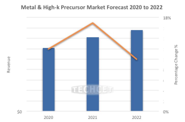
TECHCET—the electronic materials advisory firm — announced that the ALD/CVD markets will accelerate in growth due to the many new fab expansions in leading-edge Logic and Memory. As a result, the high-K and Metal Precursor markets are expected to have high growth for Hf, Co, and Tungsten precursors. The expected market is forecasted to increase 17%, reaching US$713 Million. By 2025, the market will reach US$1,050 Million. The dielectric precursor market segment will also experience high growth for the same reasons. This segment will grow 20% in 2021 to reach US$650 Million, and by 2025, is forecasted to be US$875 Million, as indicated in TECHCET’s Critical Materials Reports on ALD/CVD Precursors.

The disruptive change in NAND Flash scaling reaches upward as layered stacks have increased the demand for several CVD and ALD processes:
- PECVD dielectric stack, 32 to 192L
- Tungsten (WF6) gates
- Contacts get deeper, and stacked modules are implemented
- Multiple ALD processes within the ONO/MG stack
CVD/ALD precursor demand outgrows wafers starts because multiple new processes are added node by node for patterning and 3D-stacked scaling and replacing other deposition techniques such as PVD, Spin-on-Dielectrics, and Plating.
The industry is also getting geared up for the planar DRAM transition to 3D-DRAM, which may, just like NAND, be a growth driver for PECVD, ALD, and Etch. However, 3D implementation is on the horizon, and until then, many more nodes of continued classical DRAM scaling are being executed according to industry roadmaps. GAA-FETs will increase opportunities for Epi Si/SiGe multi-stacks. CEA-Leti has demonstrated a 7 Si/SiGe level stack and may use double exposure EUV. Current 3D-NAND scaling is good to go for 5 -years.