Contributed by Dick James, Fellow Emeritus, TechInsights
On March 8, Apple held their “Peek Performance” event, introducing the all-new Mac Studio including within it the M1 Ultra processor and its unique (up to now) packaging. We speculated in a blog after the event that Apple had used TSMC’s InFO_LSI (or CoWoS-L) silicon bridge, part of their 3D-Fabric technologies.
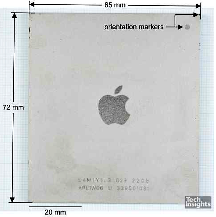
Recently TechInsights published their Advanced Packaging Quick Look report, confirming the use of a silicon bridge rather than a full interposer. As expected, the package is large, at 65 x 72mm:

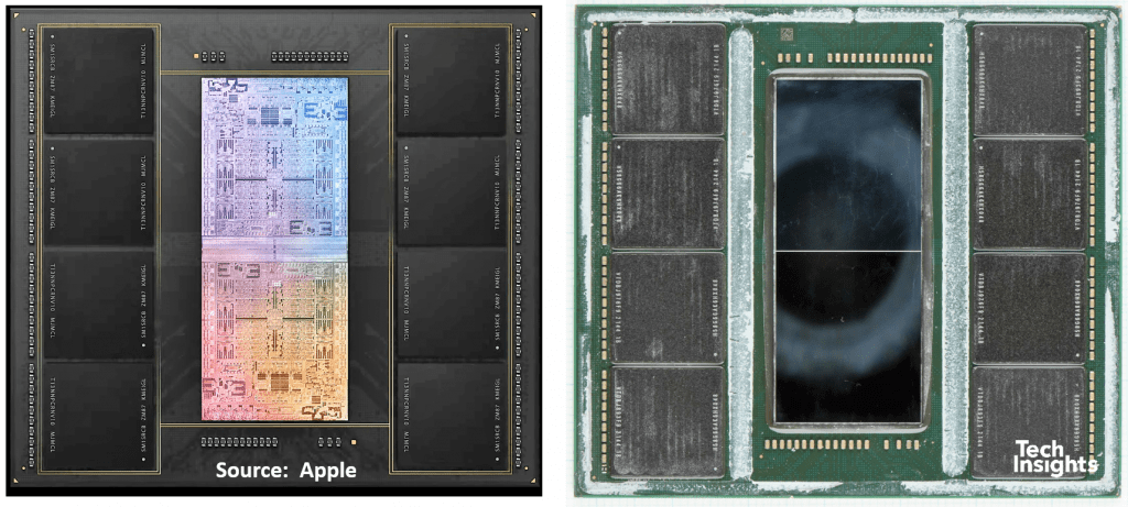
And, if we take the lid off, it matches the Apple depiction:

At the Apple event Johny Srouji (Apple’s SVP of Hardware Technologies) said “the “M1 Ultra is another game-changer for Apple silicon that once again will shock the PC industry. By connecting two M1 Max die with our UltraFusion packaging architecture, we’re able to scale Apple silicon to unprecedented new heights.” He followed up by stating that “the UltraFusion architecture uses a silicon interposer that has twice the connection density of any technology available”.
At the time we thought that a full interposer die was a bit unlikely, since even with die edge contacting die edge, a TSMC CoWoS-style interposer would be a minimum of 840 mm2. And that’s a lot of silicon, (i.e. expense), so now that we have bridge technology such as Intel’s EMIB, that seems more likely.
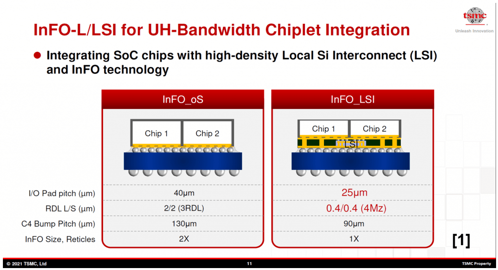

TSMC has announced two versions of a silicon bridge technology, InFO_LSI and CoWoS-L.
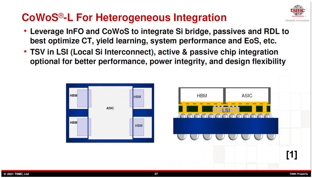

To me they look the same:
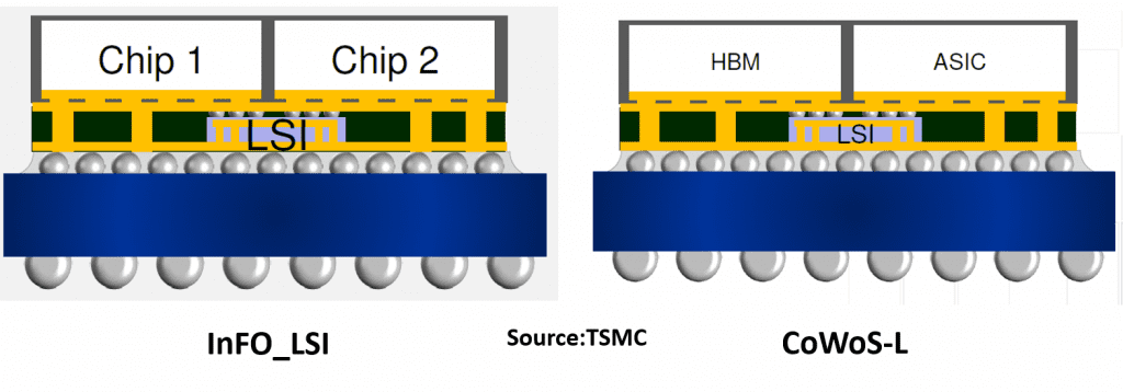

In these schematics, it looks like the bridge dies are embedded in the core of the organic substrate. But if we look at what was shown a year earlier at the 2020 Technology Symposium, we see something different:
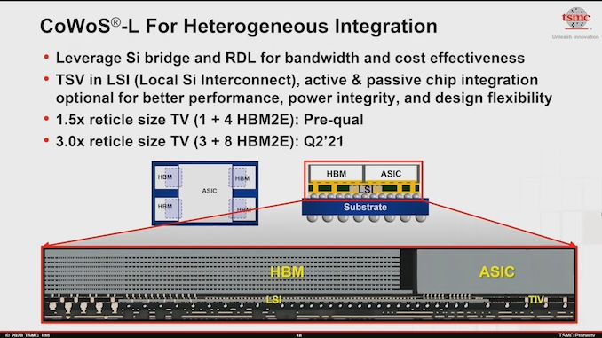

In the SEM image it looks like the LSI bridge die is sitting on top of the build-up layers in the substrate, even though the schematic above shows it embedded in the core.
The M1 Ultra looks similar, though there is no HBM involved:
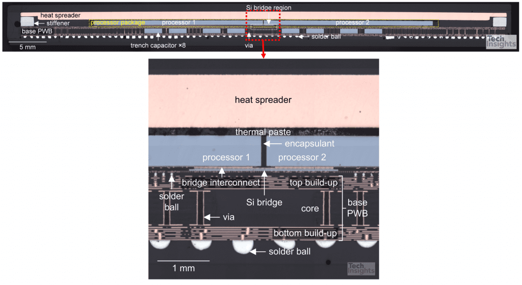

There are dies embedded in the core, but they are trench capacitor dies. The substrate itself is fairly complex with nine build-up layers on each side, connected by laser vias with large vias drilled through the core.
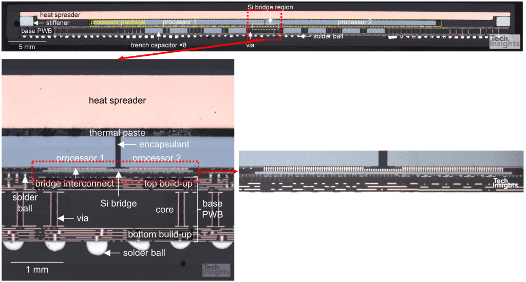


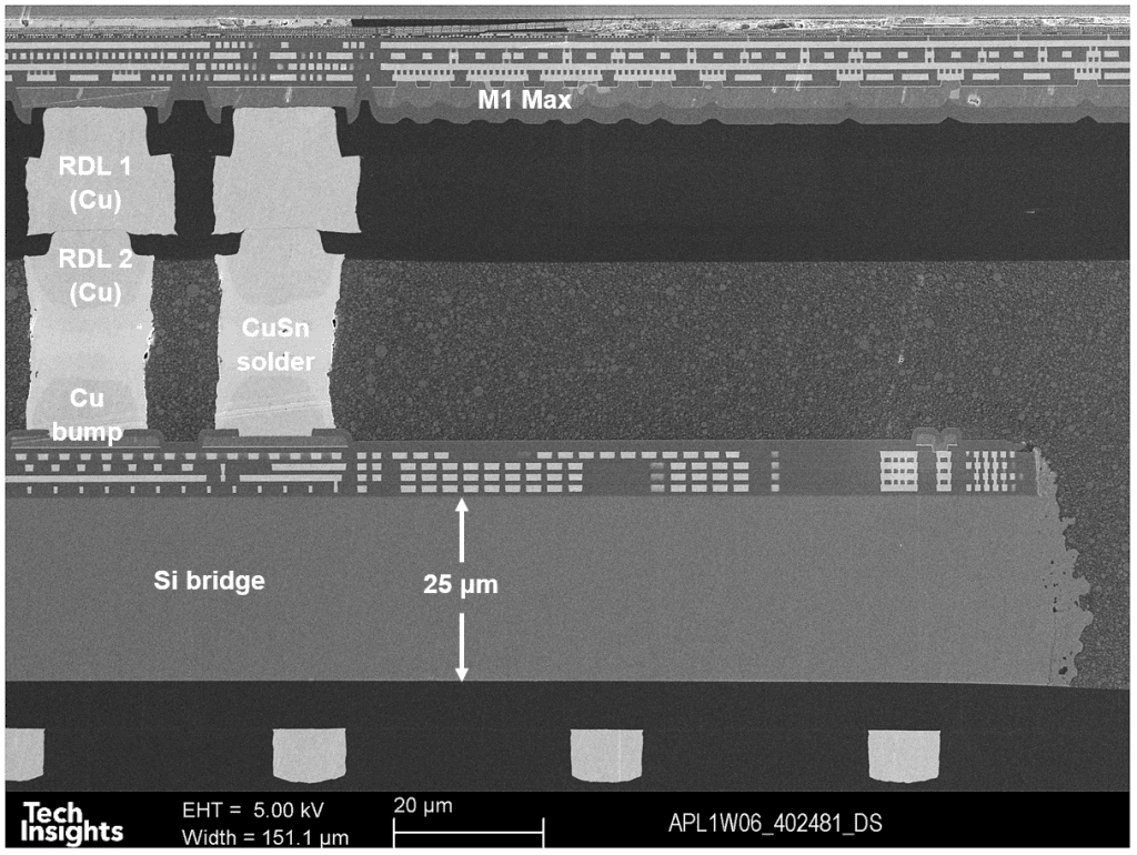
The bridge die is 18.8 x 2.88 mm, slightly shorter than the 19.05mm width of the M1Max die.
As noted in the earlier blog, bump pad pitch is 25 x 35 μm, giving a potential 57,000 total pads on the die, although Apple only mentioned 10,000 I/Os (20,000 pads).