Archer Materials Limited, a semiconductor company advancing the quantum computing and medical diagnostics industries, recently provided its quarterly update for Q2 FY24, focusing on continued development of its two chip technologies, including its 12CQ quantum processor chip and Biochip.
“The team progressed the 12CQ chip readout capabilities, including starting measurements on Archer designed readout circuits. Readout is important for semiconductors as it provides the results from quantum calculations,” said Greg English, Executive Chairman of Archer.
“The Company’s Biochip gFET designs have progressed closer to acting as a ‘lab-on-a-chip’. Archer validated its gFET designs through wafer runs with foundry partners in Germany and the Netherlands, and the team was also able to demonstrate multiplexing. Multiplexing allows the Biochip to detect multiple diseases at once on one chip.
“Continuing to build our team, developing our foundry and industry relationships, and utilizing our strong cash position will help further develop our semiconductor technologies to shape the next phase of computing and medical diagnostics.”
Qubit processor
The Archer 12CQ qubit processor chip requires high fidelity control (data input) and readout (data output) to function. Readout allows for interpretation of quantum calculations for the user, while minimizing the loss of quantum information to the surrounding environment. During the quarter, Archer’s focus involved designing and developing several quantum state readout technologies for Archer’s 12CQ chip.
Archer designed, developed, fabricated, and began measurements on its readout circuits, including devices incorporating the unique carbon nanomaterial used for the 12CQ chip. Faraday shielding for the readout devices was also designed, manufactured, and implemented. The Company completed the integration of electronic equipment to interface between readout technology and state-of-art measurement systems in facilities in Australia.
Early-stage measurements commenced on readout devices, including employing the microwave reflectometry technique. The readout devices were based on a single electron radio-frequency-box architecture and were fabricated using scanning electron microscopy and electron beam lithography. The work validated the readout device’s sensitivity to a single electronic energy level and demonstrated the tuneability of the respective resonant circuit using a varactor technology. This tuneability is significant in the context of optimizing the signal-to-noise ratio of the device’s microwave readout tone.

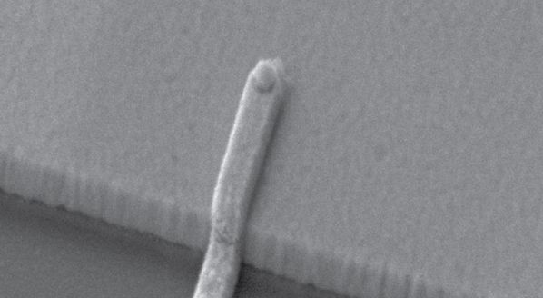
The readout devices and components required a high level of nanoscale precision between multiple fabrication steps. More advanced fabrication included the nanometer (one billionth of a meter) alignment between nanosized electrodes and discrete 50 nanometer particles of the carbon material used in the 12CQ technology (Figure 1).
The development of optimized reflectometry-based readout was awarded a UNSW Science Translational Impact Seed Funding grant to support the R&D required for the associated cryogenics and high-end electronic equipment. Archer has also gained access to an Australian- based Helium Ion Beam microscope, providing ultra-precise imaging resolution and ion beam based milling for the formation of quantum nanodevices as part of Archer’s R&D.
The Company also developed and tested low-temperature operation devices for the quantum spin state detection in few- and single-carbon nanostructures using electron spin resonance measurement techniques. Initial measurements indicated a strong correlation between the simulated and real devices. Archer intends to manufacture wafer-scale runs of these devices within a commercial foundry in the United States. The design and manufacture of readout hardware, technology, and associated techniques for the 12CQ chip is ongoing.
Archer has brought in specialist staff from the semiconductor industry, with experience developing and commercializing semiconductor products and technology. Archer is also working with commercial tier-one foundry partners in Europe for the scaled production of prototyped readout circuit and device designs, including the potential use of cutting-edge 28 nm Fully Depleted Silicon on Insulator Complementary Metal-Oxide-Semiconductor (“FDSOI CMOS”) process technology.
Archer’s Biochip
Archer’s Biochip innovation aims to integrate graphene field effect transistors (“gFETs”) into advanced fluidic systems to create miniaturized lab-on-a-chip device platforms for medical diagnostics. This could enable the ability to parallelize the detection of multiple biologically relevant targets on a chip.
The Company demonstrated multiplexing readout for its advanced Biochip gFET devices by designing and developing new hardware and software systems to readout the signal from four gFET sensors at once on a single chip. This is a significant advancement over the earlier generations of the Biochip system, which could only activate one-sensor-at-a-time, as announced on 14 September 2023. Archer intends to apply its multiplexing capability in the Biochip to test for multiple diseases on a single chip at once.
The new Biochip system with multiplexing capability also provides automated hands-free operation, as it integrates liquid handling automation and data acquisition. The software developed by Archer can display all single and time series measurements in real-time for the four gFET sensors simultaneously.
The Company validated a Biochip gFET design through a multi-project wafer (“MPW”) run by its external German foundry partner during the Quarter. The gFET device manufacturing was also the first joint fabrication between Archer and an external foundry partner, as the final fabrication processes were performed in-house by the Company in Australia.

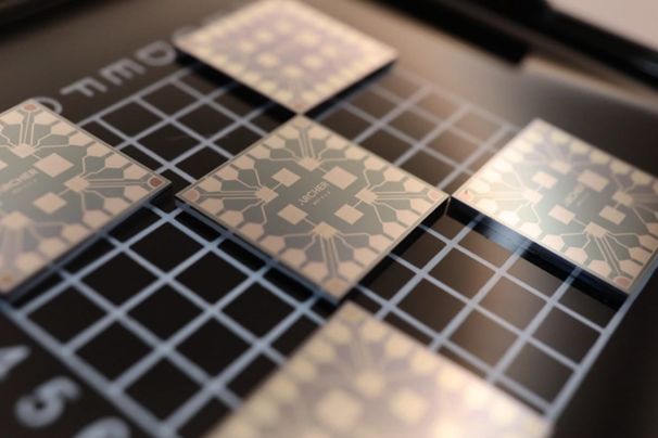
The MPW-produced gFETs were fabricated on a 6-inch wafer and diced into individual chips (Figure 2). An MPW is where Archer’s device designs are imprinted on a small area of a wafer with the designs of other companies on the same wafer. The gFET devices have been measured and function as expected, including the demonstration of liquid gating, and are compatible with the Archer Biochip system platform.
This development follows Archer’s progress on validating its Biochip gFET designs for multiplexing through a whole four-inch wafer run by a commercial foundry partner in the Netherlands. The MPW and whole wafer gFET fabrication are consistent with Archer validating its chip designs to ensure scalability for the manufacturing process of the Biochip graphene devices. Archer will use the outcomes of the runs to evaluate foundries best suited to Archer’s technology.
Archer sent a new Biochip gFET design to a foundry partner in Spain for fabrication through a four-inch whole wafer run. The foundry in Spain has ISO 13485 certification to manufacture medical device components, an important hallmark for future manufacturing partnerships. The gFETs are designed to be fabricated with structures suitable for liquid multiplexing, with advances over previous chip design features, including in gating and channel definition.
Archer plans to test the chips diced from the wafer in its laboratory in Australia, with delivery of the new gFETs anticipated in the first half of 2024. Archer is also working with the foundry partner in Spain to integrate testing of the gFET devices at the point of manufacture to improve the efficiency of the Company’s technology development processes.
By developing various designs for Archer’s Biochip gFET sensors, the Company can broaden its foundry network, improve quality control of its chips, and expand possible applications. Working with an ISO certified foundry to manufacture medical device components aligns with the nature and purpose of the Biochip, which is to potentially transform the medical diagnostics industry by providing better access for disease detection.
The Company also progressed two provisional patent applications related to the Biochip technology to patent pending by the Patent Cooperation Treaty pathway. The patent applications cover graphene field effect transistors, and a system of chip readout electronics, fluidics, and integration with liquid delivery automation and software.
Foundry and semiconductor industry partnerships
Archer continues to strengthen its relationships with global foundry partners to deliver its chips using a streamlined ‘fabless’ commercialization model. Archer is currently developing various gFET design techniques by engaging several commercial semiconductor foundries in Europe.
The Archer team recently examined the facilities of its foundry partner in the Netherlands and discussed the prospect of moving to an 8-inch whole wafer graphene process. Archer is continuing discussions with its commercial foundry partners that specialize in graphene fabrication to secure future semiconductor product manufacturing capability and to support technology development of its Biochip, including further plans for device design validations.
The semiconductor chip manufacturing processes and technology in each graphene foundry will differ, including the characteristics of graphene within the devices. Performing wafer runs in several foundries is required as part of the gFET chip development process to optimize the gFET design and manufacturing for foundry readiness and compatibility.