The ending of the Cu era?
Since its introduction in the mid-1990s, copper (Cu) has been the mainstream conductor metal for fabricating interconnect lines and vias in logic back-end-of-line (BEOL) applications. Through the years, the conductivity and reliability of Cu in dual-damascene integration schemes have remained unbeaten, so there was no need to replace this champion metal in interconnect applications.
But with each new technology generation, the local metal layers continue shrinking and soon, the most critical ones will be barely 10nm wide or even less. Unfortunately, at these small dimensions, the resistivity of Cu increases dramatically, impacting the performance of the electronic circuits.
On top of that, Cu needs a barrier, a liner, and a cap layer to ensure good reliability. These extra layers minimize out-diffusion into the surrounding dielectric (and hence, the risk for dielectric breakdown) and ensure good adhesion. The thickness of these layers (with typically high resistivity) does not scale well with the interconnect line dimensions. Consequently, they occupy an ever-increasing part of the metal volume without contributing much to the conductance.
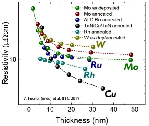
The worrisome behavior of Cu conductors at small dimensions forced the interconnect community to start looking for alternative metals in combination with new metallization schemes. Initially, the spotlight was on pure metals – the simplest of possible conductors – and their database has been well-documented. An interesting observation is that the industry’s standard is predicted to behave the worst at small dimensions, with better forecasts for e.g., cobalt (Co), ruthenium (Ru), rhodium (Rh), iridium (Ir), and molybdenum (Mo) [1]. At larger dimensions, the resistivity of these alternative conductors is higher than the one for Cu. But, because their resistivity increases more slowly when interconnect dimensions are reduced, they have better prospects at smaller dimensions. However, several of them do not turn out favorably when we consider, for example, raw material cost and environmental impact.

Looking beyond pure metals: a new field of research
About five years ago, imec decided to broaden its search towards compounds. The starting point: can we find binary and/or ternary ordered compounds (intermetallics) that, at small dimensions, do better than Cu (and other pure metals) in terms of resistance and reliability? And which ideally do not require a diffusion barrier or adhesion liner? The first results of this seminal research announced at the 2018 International Interconnect Technology Conference (IITC 2018), were very encouraging [2]. Since then, several R&D groups worldwide have embraced the idea and are looking for candidate alloys, focusing today on the binaries [3, 4, 5].

However, the search for new metals is not easy, with numerous challenges to address. Above all, the list of possible material combinations is enormous, and the properties of many metals in small dimensions have not been studied in detail. Often, not even detailed bulk properties have been reported. So what is the best way to shorten the list before we can even think about doing experiments? How can we be sure that our choices are sustainable and cost-effective? And are these alloys stable and compatible with real metallization schemes?
This article presents a refined and unique methodology for shortlisting and ranking the candidates based on ab-initio calculations, experiments, and modeling. Next, we address the potential materials and discuss the next steps, i.e., their implementation in advanced metallization schemes.
Atomistic calculations narrow down the number of candidate alloys
Well over 5.000 material combinations can compose conductive binary alloys and even more can synthesize ternaries. Therefore, some guidance is needed to accelerate the development and provide a meaningful down-selection. For example, looking only at the (bulk) resistivity is too narrow, as the conductors might behave better in confined areas.
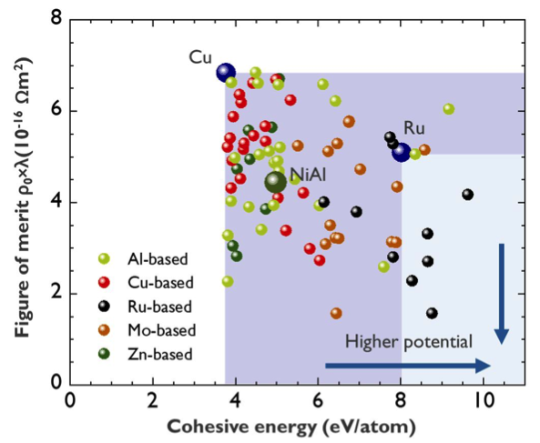
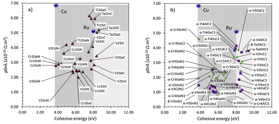
Therefore, the first step in selecting and ranking the most promising materials is identifying the most relevant figures of merit to benchmark against Cu. The imec interconnect team proposes two figures of merit: the cohesive energy and the product of the bulk resistivity and the mean free path of the carriers.
Resistivity x mean free path – to predict the resistivity increase at small dimensions
For future interconnect applications, both the metal’s bulk resistivity and the carriers’ mean free path within the metal should be as low as possible. The smaller the mean free path of the carriers, the less they will be subject to size-dependent scattering by surfaces or grain boundaries that occur in scaled interconnects. Therefore, a smaller mean free path forecasts a smaller dependence of the resistivity on the interconnect line dimensions.
Although both parameters are key indicators, for ease of calculation, we use the product of the bulk resistivity and the mean free path as a figure of merit for a first down-selection. To qualify as a future interconnect metal, the value of this product should be better than that of Cu, which has a bulk resistivity of 1.7µΩcm and mean free path of 39nm (at room temperature).
Cohesive energy – as an indicator of intrinsic reliability
The second figure of merit, the cohesive energy, serves as a proxy to assess the reliability of the conductor in interconnect schemes. The reliability of interconnect lines is typically affected by two phenomena. First, conductors may suffer from electromigration, which refers to the drift of metal ions due to for example large charge currents, or diffusion of atoms due to heat, or stress gradients. Furthermore, some of the metals tend to diffuse into the surrounding dielectrics. Without any barrier, this can lead to dielectric breakdown. Both phenomena depend on how easily the metal atoms are detached from the interconnect material, a property that the metal’s cohesive energy can capture. For Cu, this value is ~ 4eV.
Both figures of merit can be derived from atomistic calculations based on a solid-state physics description of the material’s electronic structures, and the results from these “ab-initio” simulations are visualized in a benchmarking graph. Only those alloys with comparable or higher cohesive energy and lower bulk resistivity x mean free path than Cu are selected for further (experimental) work.
Before moving on with this selection, other considerations come into play. For example, how well do these alloys adhere to the dielectric? Do these compounds exist in (thermodynamically) stable phases? And if we need any annealing steps to enable those stable ordered phases, are the temperatures compatible with BEOL processing? Do the alloys contain any toxic or rare compounds? And what about the material cost? Further insights into the materials science allows us to down-select some of the material combinations from the obtained list of candidates.
Experimental work to further assess the scaling potential
The ab-initio-based sub-list is the starting point for further experimental work on 300mm wafers to verify the theoretical findings. The gained data are also used to feed the modeling work and better understand the conductors’ behavior at small dimensions.
In one series of experiments, the researchers deposit blanket thin films with varying film thicknesses and measure the resistivity of the films. In a second series, test vehicles with patterned t-shaped structures – relevant for interconnect applications – are created to investigate the scaling potential in narrow lines. Some of the material combinations will have a higher bulk resistivity than Cu. To remain in the candidate list, this value may not be too high, and their resistivity should increase slower than the one of Cu, with cross-over points around 10nm (or higher) – the dimension where Cu starts to become problematic.
These experiments also give us an idea of the accuracy gained with the ab-initio-based method for shortlisting.
Identifying the candidates: from binary aluminides to ternary MAX phases
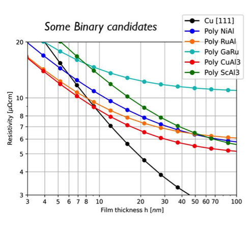
The ab-initio simulations have shown promising properties for various binary alloys, including Al, Cu, and Ru-based compounds – although not the only candidates. Today, the resistivity behavior of these binary alloys is being investigated experimentally by research groups worldwide. In 2019 and 2020, Asian and American research groups reported on their progress [3, 4, 5]. At IITC 2021, imec reported further results on the resistivity of thin films of aluminides using 300mm substrates, including AlNi and AlCu [6]. While the worldwide effort is also an illustration of the need for new conductors and clear progress has been made, there are still significant material and integration challenges ahead.

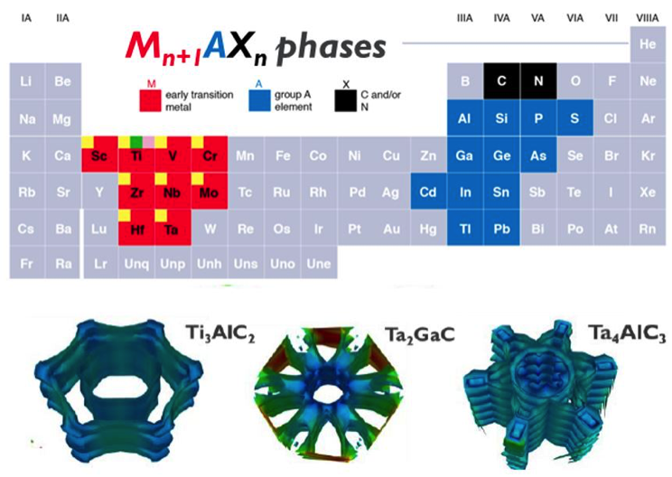
Our team also considered more complex ternary compounds. For ternaries, however, the number of possible combinations is so large that even an ab-initio pre-screening is not possible anymore. The properties of most ternary compounds are unknown, even if they are metallic. Therefore, we must select certain material classes that are already studied, e.g., the MAX phases. MAX phases are layered structures composed of an early transition metal (M), an A-group element (A, columns 13 or 14 of the periodic table), and carbon or nitrogen (X). Some of these MAX phases are expected to do better than the pure elements, providing an opportunity for further research. [7, 8].


The test vehicles with patterned structures do not fully grasp the complexity of integrating the alloys in real interconnect modules. For the near future, the team is therefore preparing to move to the next step: implementing the most promising candidates in relevant metallization schemes and addressing the challenges related to BEOL processing.
The alternative metals are aimed for introduction in the most critical (local) interconnect layers as a far-out option. Imec’s BEOL roadmap foresees their implementation using a semi-damascene interconnect module, which involves the direct etching of a patternable metal to achieve high aspect ratio lines [9]. Note that for upper interconnect layers, Cu is expected to remain the metal of choice.

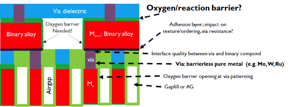
Implementing the selected binary and ternary compounds in these semi-damascene modules will reveal the challenges of true interconnect integration. For example, we identified the control of the film stoichiometry and surface oxidation to be the first challenges to address. Subsequent experiments should also allow to optimize the etching strategies needed for the metal patterning.
In the future, these research activities will expand with sustainability assessments. While supply chain risks and costs can be evaluated earlier in the exploration phase, assessing the environmental footprint of the process flows requires more detailed knowledge of the different process steps. This includes, for example, more insights into the chemistries needed to etch the new conductors, the required annealing steps, the biproducts needed for their formation, etc.
Conclusion
The search for alternative binary and ternary metals for future interconnect applications, initiated by imec about five years ago, has become a new field of research with worldwide interest. In this article, we described a unique methodology that provides guidance to down-select and rank the possible candidates. The methodology starts with calculating two main figures of merit and is complemented with experimental and modeling work. Using this method, several binary and ternary (MAX) alloys have shown promising properties, providing an opportunity for further research.
Want to know more?
[1] ‘Molybdenum as an alternative metal: thin film properties’, V. Founta et al., IITC 2019;
[2] ‘Alternative metals: from ab initio screening to calibrated narrow line models’, C. Adelmann et al., IITC 2018;
[3] ‘The search for the most conductive metal for narrow interconnect lines’, (invited perspectives article; also: Editor’s pick: “Featured Article”)’ D. Gall, J. Appl. Phys. 127, 050901 (2020);
[4] ‘Materials for interconnects’, D. Gall et al., MRS Bulletin, October 2021;
[5] ‘Intermetallic compounds for interconnect metal beyond 3 nm technology node’, J. Koike, IITC 2019;
[6] ‘Imec introduces intermetallics and airgaps in advanced interconnect metallization schemes’, imec press release 2021;
[7] ‘Metallic ceramics for low resistivity interconnects: an ab initio insight’, K. Sankaran et al., IITC 2018;
[8] ‘Ab initio screening of metallic MAX ceramics for advanced interconnect applications’, K. Sankaran et al., Phys. Rev. Materials 5, 056002 – Published 24 May 2021;
[9] ‘Logic technology scaling options for 2nm and beyond’, imec reading room 2021.
Interested in receiving one of the imec IITC contributions? Fill in our contact form.
About the authors


Geoffrey Pourtois joined imec in 2003 and has been working since then in the field of atomistic modeling, with a special attention for establishing relations between material, interface defects and electrical device performances. He obtained a Ph.D. degree in Chemistry in 2002 from university of Mons Hainaut, Belgium. From 2003 to 2022, he has been building and heading the material simulation and physics group within imec, where he and his team have been focusing on the modeling using atomistic simulations of nanoelectronic related materials, and on complex material gate stacks, touching different aspects bound to it such as the identification of new metal candidates for interconnect, emerging and magnetic memories; 2D materials; doping strategies for transistors; CMOS metal gate work function engineering; identification of transparent amorphous semi-conductors; the modeling of mechanical and thermal properties and the identification of atomic layer depositon precursor for material growth. In 2020, he was nominated imec fellow.


Christoph Adelmann, Ph.D. joined imec in 2006 and has been working since on materials and processes in numerous fields, including high-k dielectric, metal gates, dielectrics for nonvolatile memories, III-V transistors, and novel metals for interconnect. He obtained a Ph.D. degree in condensed matter physics in 2002 from Université Grenoble Alpes, France for work at the CEA Grenoble. From 2002 to 2006, he was a postdoctoral research associate at the Department of Chemical Engineering and Materials Science at the University of Minnesota, working on spintronic materials and devices. At imec, he is currently a Scientific Director driving research on advanced metals for interconnects, magnetic devices for memory and logic, as well as the characterization of 2D materials.


Zsolt Tőkei is imec fellow, and program director of nano-interconnects at imec. He joined imec in 1999 and, since then, has held various technical positions in the organization. First, as a process engineer and researcher in the field of copper low-k interconnects, then headed the metal section. Later he became principal scientist, and program director of nano-interconnects. He earned a M.S. (1994) in physics from the University Kossuth in Debrecen, Hungary. In the framework of a co-directed thesis between the Hungarian University Kossuth and the French University Aix Marseille-III, he obtained his Ph.D. (1997) in physics and materials science. In 1998, he started working at the Max-Planck Institute of Düsseldorf, Germany, as a post-doctorate researcher. Joining imec, he continued working on a range of interconnect issues, including scaling, metallization, electrical characterization, module integration, reliability, and system aspects.