By Dick James
In the field of reverse engineering, TechInsights is the world’s leading provider of analyses of advanced technology and associated intellectual property services to many of the world’s most successful technology companies.
Founded in 1989, and headquartered in Ottawa, Canada, TechInsights has over 380 employees, with offices around the world. The company tears down and analyzes over 750+ consumer products per year and catalogues over 6,500 components per year, as well as analyzing over 2,000 chips. Analyses go from the system level, right through to the silicon.
The majority of the products from TechInsights are subscription-based into different channels, from detailed teardown reports of commercial products, through to the performance characteristics of the latest 5-nm transistors. In my career there I was mainly concerned with semiconductor process analyses, so naturally my interest is in the process reports.
The leading-edge devices that push the limits of transistor performance are covered in the Logic group of analyses, with channels such as Process & Advanced Packaging, Process Flows, and Transistor Characterization.
A few months ago, TechInsights concluded that there is a lot of information that gets lost in the continuous sequence of individual device reports and scheduled analyst summaries, particularly in the details of transistor construction. While competing devices can come on the market with fairly close timing, and we can make the comparison then, it is more difficult to follow the technology evolution as new nodes bring in new developments.
Consequently, it seemed like a good idea to generate compilation reports, where we track the changes in transistor architecture across the generations and review the trends that are revealed. These compilation reports are now available in a new Technology Architecture Comparison Channel.
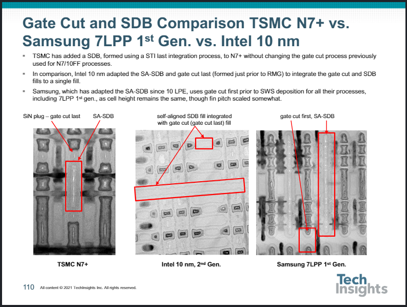
The latest is a comprehensive comparison of TSMC, Samsung, and Intel FEOL development, from the Intel 22-nm introduction of the finFET through to 10/7-nm technologies from the three leading-edge manufacturers.
So far, we have ten in the catalogue for this new channel:
- TSMC channel architecture comparison, 16FF – 7FF (sample)
- TSMC gate technology comparison, 16FF – 7FF
- TSMC source/drain (S/D) comparison, 16FF – 7FF
- Samsung gate technology comparison, 14LPP – 7LPP
- Samsung channel technology comparison, 14LPP – 7LPP
- Samsung source/drain (S/D) comparison, 14LPP – 7LPP
- Intel gate technology comparison, 22 nm – 10 nm Cannon Lake
- Intel Channel Architecture Evolution, 22 nm – 10 nm Cannon Lake
- Intel Source/Drain Architecture Evolution, 22 nm – 10 nm Cannon Lake
- TSMC/Samsung/Intel Logic FEOL Process Technology Evolution
Nine out of ten of the reports detail the evolution of the specific processes through the generations, from the specific companies, highlighting the changes and filling in some of the gaps not covered in the regular device report format or the analyst summaries. As you will have gathered, the latest is a compilation of compilations, covering all three companies.

Within each topic the discussion is broken out by company, comparing the generations, with a summary page showing the essential differences and similarities of the three suppliers.

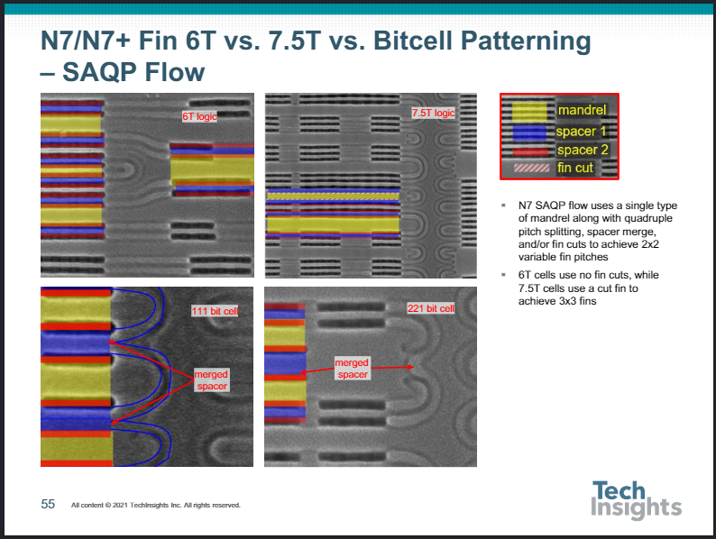
A more focused example is this detail of the TSMC patterning for 7.5T cells vs 6T cells:

We could list much more of the focused content, but that would over-lengthen this blog unnecessarily. With this report the customer can review a concisely curated summary of the evolution of the front end over the finFET nodes from the first generations of TSMC, Samsung, and Intel.
The more focused reports on the individual companies gave the authors the opportunity to go back and review the full library of images, add in more detail, and fill in possible stages that were performed but removed as part of the fabrication sequence.
In short, these additional reports in the new Technology Architecture Comparison Channel are a fresh look at the data, and a valuable addition to both the single device process reports and the regular analyst summaries. More details of this and the other Logic channels are available on the TechInsights website.