The cost of many 300mm Chemical Mechanical Planarization (CMP) consumables has decreased in recent years due to a maturing market and new process learning, making it economically feasible to embark on a new 200mm Oxide CMP polishing process based on these advanced commercial consumables in the market, today. But to bring new CMP consumables into production, a variety of polishing pads and conditioner disks, optimized process settings, and unique tool limitations need to be screened.
In this case, study to demonstrate opportunities for back qualification to 200mm processing, challenges for this screening process included:
- Using a Mirra-Standalone™ Polishing process for benchmarking
- Low cost of ownership and high yield
- Reduced qualification time, less than six months
- Numerous consumables vendors to test
Despite challenges, such an endeavor presents the benefits of developing a new process, including a new low cost, high rate, and low defectivity process that provides an increase in pad/disk life, head life, and tool throughput while maintaining a world-class Mean Time Between Failures (MTBF) of 48 hours. This shift can result in a higher fab output and lower customer returns due to reduced CMP induced defects.
Tends driving CMP process development
The recent economic upturn that our industry has experienced over the last few years has resulted in some developments. [1] Many fabrication facilities had to increase employee headcount and curtail spending, all the while dealing with higher wafer output.[2] This effect trickled down to the semiconductor consumable vendors, they, in turn, upsized as well.
In early 2016, semiconductor fabrication sites received emails from their CMP pad vendor that they may not have enough supply due to higher demand. This pad shortage left semiconductor fabs with few options.
Some CMP manufacturing teams proposed developing a process based on the new third generation pads on the market for 300mm fabs due to some economic and logistical reasons. The first rationale for this strategy was cost and second was time; most of the pads on the market were considerably less expensive than the current process of record pads for the 200mm fabs. Because they are back qualifying the higher node 300mm consumables down to the 200mm size fabs cut down on the development and expense of starting from scratch.
Keys to success
There are three main reasons that a fab might succeed in developing an Oxide polishing pad process in a short amount of time, including 1) detailed engineering work; 2) management support; and 3) strong vendor support.
Process development can go through three generations of refinement before it is ready for high volume manufacturing. The first version focuses on new pad improvements such as third generation high rates, low defects pads designed for lower technology nodes and an array of the design of experiments, continuous improvement through optimization of process controls and equipment modification followed in the second revision. The third generation can attempt to adopt existing Mirra tools using a previous qualified process. A final successful attempt can be made during the third cycle to develop a lower cost, higher throughput, low defect polishing pad process.
How a new polish pad process was designed and qualified
Polishing pads are made up of hard polyurethane top pads with soft sub-pads — the first generation application on most oxide back end of the line CMP process. The pad is dependent on a semi-rigid hard polishing pad, high cut rate conditioners and mechanical in nature oxide slurry removal profiles. The pads can also be very high in cost and low in consumable life compared to the most conventional CMP process. i.e., Tungsten, Shallow Trench Isolation (STI).[3]
This process of record (POR) was no different; a first generation oxide pad used to abrade the oxide from the wafer surface. The consumables were short in life due to high process temperatures, long conditioning times and the aggressiveness of the fumed silica slurry, not to mention the high cost of ownership ( i.e., slurry cost, short pad/disk/head life).
Pad identification
To reduce time to develop a new Oxide Polish process, most of the development cycle could focus on polishing pads leveraging existing slurry’s, conditioning disks, and heads. To achieve maximum throughput, the wafers would need to be processed through the tool’s three platens with equal polish time. To set up this case study, it’s important to understand the major players in CMP polishing pads. Each pad vendor should be asked to obtain information to prepare a white paper screening to determine the correct path to go down since time was short. Candidates need to be evaluated on pad type, makeup, SG, cost, and compatibility to current slurry and tools.
In this instance, two of the pads fit the bill for the criteria and selected for further testing. Pad A, similar to the current POR and was from the current pad Vendor; Pad B was a novel approach for Oxide CMP and was from a new pad vendor on the market that previously only supplied pads to 300mm fabs. It had an advanced thermoset cast top pad, a reduced wicking sub-pad and adhesive durable in high temperature and shear.
To meet the tighter requirements on some devices, two new oxide pads were identified for qualification. The initial criteria used to judge the pads were blanket test wafer performance (Teos, and HDP and doped Teos), including:
- Removal rate
- Nominal removal profile
- Removal profile tunability via recipe parameter windowing
- Defectivity
Experimental designs (DOE’s) were run on the basic process controls with these pads to evaluate:
- Carrier speed
- Table speed
- Down-force
- Carrier position
- Carrier oscillation
- Slurry flow
Both pads performed well on the blanket experiments and advanced to short loop, patterned wafer tests; these patterned wafer tests were used to study product removal rate behavior and over-polish windowing.
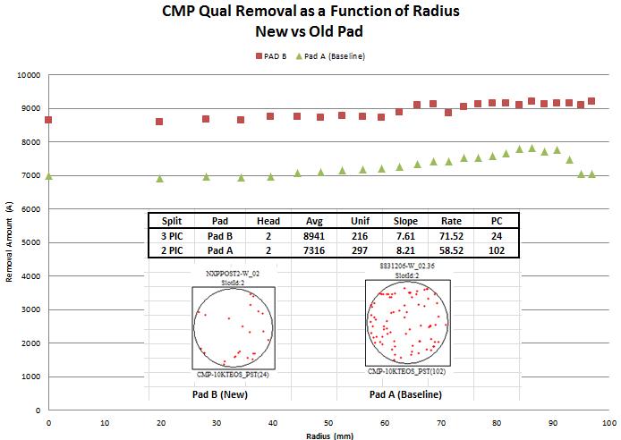
A significant amount of time was spent adjusting recipe parameters to eliminate edge removal roll-off (especially at the wafer’s extreme edge, 96mm) and to achieve uniform and reasonable polish profile performance, (Figure 1). Both vendors were contacted to do lifetime experiments with consumables at their facilities and the data collected revealed many challenges with each candidate.

Pad A was first generation polishing pad that had a hard polyurethane surface sandwiched with a soft sub-pad, still a very Prestonian mechanical process. The overall polish profile was sufficient but would degrade after about 400 wafers on the pad causing higher defectivity due to temperatures spikes and lower consumable lifetimes across the three platens. This pad was disqualified due to this reason.
Pad B was a third generation pad that had a low durometer in nature, soft landing features, and was developed for 15nm manufacturing technology nodes. This pad was commercially available to 300mm fabs only, but manufacturing adjustments were made to introduce it in a 200mm fab setting. This pad offered a new spider web grooving pattern to enhance slurry flow. It had a higher removal rate compared to the baseline but demonstrated much lower overall defectivity throughout the pad lifetime; it also showed lower process parameters. [4]
The one problem with this pad was with the premature pad balding which was overcome by multi-DOE runs looking at process parameters offsets. The outcome was to reduce the conditioner down-force and time, with such a soft pad it was not wearing the conditioner diamonds and degrading the cut rate of the pad, unlike the POR. This pad was the optimal solution for qualification. (Figure 2)

Vendor support
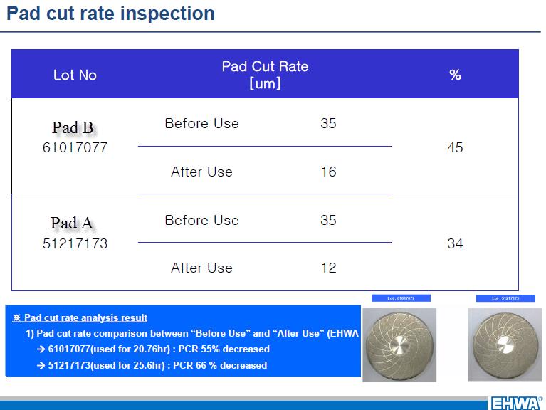
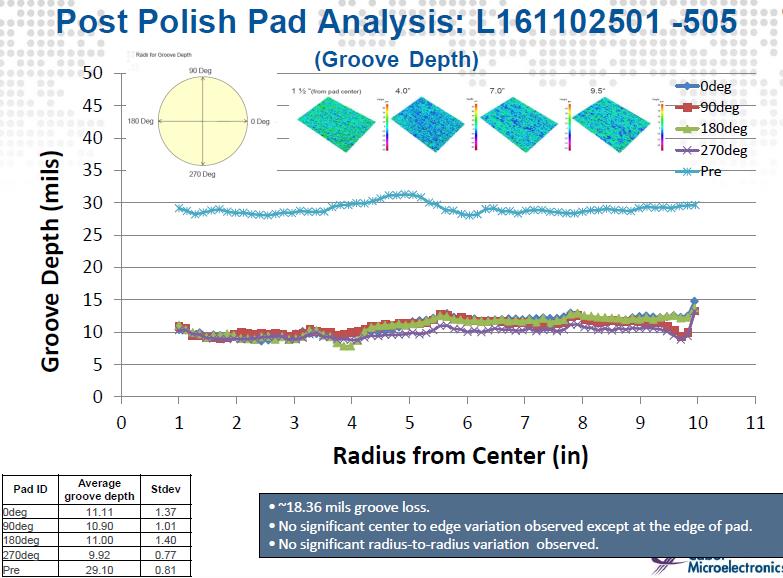
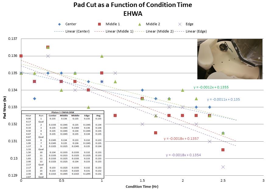
The fabs internal polishing engineering staff was augmented with exceptional support from several consumable vendors during development. Together the fab engineers developed proprietary and patent-pending technologies to enhance the Mirra performance on oxide back end of the line CMP. The Team also benefited from strong relationships with its pads and conditioning suppliers. To improve the tool’s performance, EHWA™ conditioners were pivotal in adding additional functionality to the process thru the end of life evaluations. A mini-DOE was run to understand pad cut rate based on conditioner downforce. (Figure 3) Perhaps most important of all relationships that developed was with Cabot Microelectronics™, who provided an invaluable education into pad process development. Many conditioning process changes were run to reduce the final pad groove depth thickness profile, to extend pad lifetime, Cabot Microelectronics Engineers were instrumental on pad ware analysis. (Figure 4)


Defect concerns
During process development, a fab engineer could encounter several defect related issues, and two may take more troubleshooting: Pad balding, Micro-scratching.
The presence of pad balding would shorten lifetime and cause higher defects. Due to the limited knobs on the AMAT Mirra Conditioners to adjust the tool’s cut profile, Oxide polish engineers would need to work closely with conditioner vendor engineers to produce custom disk based on specific requirements and may need to run extensive pad cut-rate tests. Pad cut rate was achieved by cutting small holes in the pads at a different radius from the pad center, then using a drop micrometer to determine pad height measurements while running different conditioner settings, i.e., downforce, dwell time and time in zones. These experiments can show that the new pads did not need much conditioning to maintain high removal rates and low defectivity. (Figure 5)
With pad balding effectively eliminated, the next major technical challenge may be micro-scratching. A Process Of Record (POR) uses fumed silica slurry because the process lacked a final table conditioner, its soft pad would become progressively more and more embedded with slurry, effectively becoming fine sandpaper. This can cause excessive micro-scratching of the wafer which required pulling the buff pad early in a lifetime.
While micro-scratching in of itself was not a significant yield concern, the saturation of defect scans masked true killer defects and therefore is unacceptable. To solve this problem, a completely different pad employing different manufacturing and other proprietary components can be tested and qualified. The new pad may eliminate the silica embedding problem entirely and as a result pad lifetime can increase which will reduce consumable age and test wafer expenses but most notably dramatically increased tool availability.

Further process development
One of the last stages of development on the new process is a project to develop a faster throughput process. The motivation for this work is to boost the throughput and further cut process expense dramatically. To maximize throughput, the new process would have two components: Each wafer run would have no more than 45 seconds dedicated to platen 1, & 2 processing and 115 seconds of wafer loading/unloading while in-situ conditioning occurred.
The final platen process was integrated with the other platens (same pad and disk). Therefore, distributing the time equally between the three platens. The polishing composition of this work is surprisingly good. Because of the high down forces employed to achieve a flat removal profile, dishing on large pads tended to suffer regardless of the process used. On the other hand, erosion tends to be quite reasonable. Perhaps most impressive of all is the erosion uniformity which when measured by High-Resolution Profilometry (HRP) from center to edge, was consistently achieved at less than one sigma.
Benchmarking performance
For initial qualification and benchmarking was installed and set up the best-known method (BKM) three platen polishing process on an Applied Materials Mirra ™. To bring the new process into production, Oxide Polish engineers were tasked with demonstrating equivalent or better yield between the two competing processes. With such low dishing and erosion amounts on the new pad, the product end of line testing may be higher than the baseline (Flatter Profile, less edge roll-off), but within control.
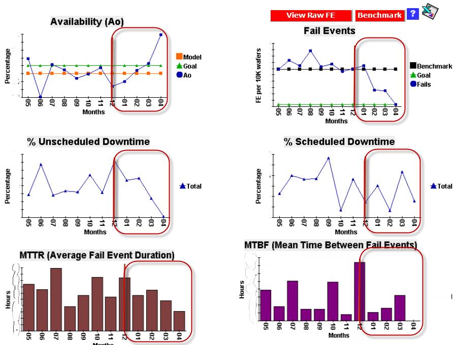
After extensive electrical and yield testing, the new three platen process was fully released. Sample yield comparisons between the two processes consistently demonstrated that performance is equivalent to slightly better and the new process has higher thru-put (~20%). The consumable costs (slurries, pads, conditioners, etc.) are 17% less per wafer pass than the competing process. The pad/conditioner life increased by 25% from the previous process due to reduced conditioning down-force. Head lifetimes increased by 13% due to lower process parameters that reduced retaining ring ware; this in-turn reduced the amount of head load/unloads failures that increased the MTBF of the tool from the low 30 to high 40. (Figure 6)

Conclusion
A three platen oxide polishing process may be developed using new third generation low abrasive polishing pads. Despite some tool’s many limitations, a strong engineering staff can successfully deliver an integrated process capable of producing equivalent yield at substantially lower costs over the best alternative method.
Undertaking such a task undoubtedly presents challenges, only a fraction of which have been described in this article. By leveraging an existing deep reservoir of engineering, maintenance, and operational talent, an existing and efficient supply chain, and the outstanding support of numerous vendors, a Fab CMP module may be able to realize its goal of making efficient use of its assets to achieve a competitive advantage. The value to the customer would show to be the lower overall cost of ownership and higher throughput.
CHRISTOPHER ERIC BRANNON is a TI Cu CMP Manufacturing Engineering, Texas Instruments, Dallas, TX.
References
-
Stefan Heck, Sri Kaza, Dickon Pinner ‘Creating value in the semiconductor industry’ Mckinsey & Company
- James Carbone ‘Semiconductor market will recover in 2017’ Electronics Sourcing
- Che-Chin Yang, Kai En Lin, Wei-Nan Fang ‘Planarization improvement using a non-porous polishing pad in ILD CMP’ ICPT 2015 International Conference on CMP
- ‘Nexplanar® Advanced Pad Technology’ Cabot Microelectronics 2016
- ‘Analysis Report of Returned Disc.’ Feb. 17, 2017, EHWA Diamond
- ‘Post Polish Analysis’ Feb 28, 2017, Cabot Microelectronics