HARIS OSMAN, imec, Leuven, Belgium
Most chips today are designed and fabricated in standard CMOS technologies. But much more is possible with fully customized chips, resulting in creative solutions for customer challenges. Some examples include ultraviolet light or low-energy electron detectors, image sensors with postprocessed filters, labs-on-chip with microfluidic channels, and chips with integrated photonics components.
But designing these specialty chips requires a multidisciplinary approach. Further, to convert concepts and prototypes into reliable products that meet customer specifications requires a well-oiled, veteran industrialization team.
Imec is one of the world’s premier R&D fabs, working with major semiconductor companies to enable their technology roadmaps. We accomplish this by continuously thinking out of the box, and evaluating a broad range of new materials, technologies and process architectures. Simultaneously – in contrast to university labs, for example – we keep an eye on industrialization, and the attainability of reliable fabrication with our current industry tools.
Our scientists have developed multidisciplinary expertise and the know-how to industrialize solutions. With the combined wealth of experience, we can tackle some of our partners’ needs for custom-made chips.
A defining challenge was the one ASML gave us. ASML builds the lithography systems that allow chip producers to pattern the small features of today’s chips. Their lithography system uses extreme ultraviolet light (EUV) and combines over 100,000 innovative components, most of them unique. One of these components is a sensor chip that measures the dose of incident EUV light. ASML managed to build a prototype of such a sensor in 2011. However, they did not have the capability to fabricate these sensors in the quality and volume that they needed. As they already knew us as a trusted partner, they came to imec.
ASML is just one example of a trend of companies increasingly wanting to deploy specialty chips. If it’s a completely customized chip which needs a multidisciplinary approach, and which needs to be fabricated in small but highly reliable volumes, imec is one of the few places that can deliver.
Toolboxes to mix and match
To produce solutions faster and to consolidate our expertise, we’ve developed a number of platforms. These are versatile and robust toolboxes of modules that are continuously maintained and improved.
To design a custom solution, our teams use these platforms as a basis, and mix and match process modules to arrive at the best solution. Examples of such toolboxes are advanced MEMS, photonics, microfluidics, specialized image sensors, and wafer-based post-processing of filters.
One recent example of a unique imager toolbox that we’ve developed is our time-delay-and-integration (TDI) CCD-in-CMOS technology. TDI imaging is a high-quality line-scanning technique used in applications such as industrial inspection and earth observation. It is used when an object or scene is moving linearly under the imager. We decided to use a CCD to collect and transfer the pixel data, even though a full CCD system traditionally requires a board with multiple chips, including a CCD chip, drivers and readout chip. This is a typical example of a case where there was much to gain with further integration.
Imec developed a new solution that combines CCD pixels and a CMOS readout in one technology, enabling a single imager chip with both CCD and CMOS functionality (Figure 1). This unique technology combines the best of two worlds: the high-quality pixel collection and transfer of the CCD technology, and the system integration, low power usage and fast readout that only CMOS can deliver.

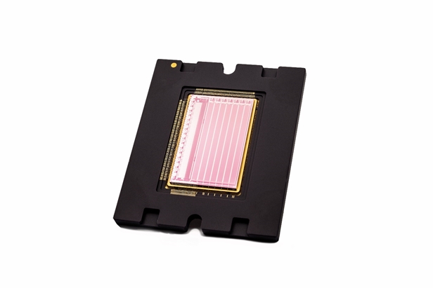
With this new CCD-in-CMOS capability, we can now begin to offer customers compact and superfast TDI solutions.
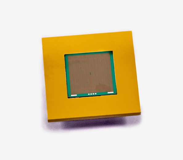
Another example, one where we used our microfluidics capability is our own miniature microfluidics heat sink for high-performance chips (Figure 2). In this silicon cooler, we made microchannels that were 32µm wide and more than 260µm deep. Through these, a coolant liquid is pumped that can dissipate more than 600W of heat per square centimeter, keeping the chip temperature below 100°C.

From idea to prototype to product
Companies come to us with diverse, challenging problems for which they find no obvious answer in standard foundries. To satisfy our customers’ needs – idea development and research, product or prototype fabrication, design process synthesis, or something entirely unique – our engineers use imec’s diverse toolbox of skills and platforms.
Our customers have two main concerns when they collaborate with us. First, whether we’ll be able to come up with a solution that meets their specifications. Second, they want to know that we’ll be able to supply the chips in a timely manner. Often, their whole time to market depends on our specialized component, so there is huge time pressure to deliver.
That is why we have set up an industrialization team, who have strong industry experience. This team takes up the prototype process and will start to make it more controlled and standardized, resulting in a process that can be run reliably, with predictable yield. This will guarantee the timely supply of chips to customers.
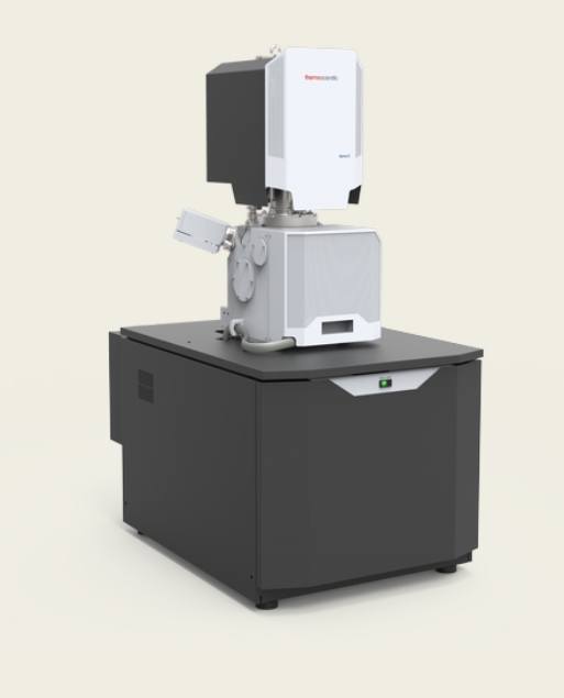
This is exactly what we’ve been doing for FEI Company, a subsidiary of Thermo Fisher Scientific. FEI is a market leader in scanning electron microscopes (SEM) – Figure 3 — and they asked imec to make an electron detector according to their custom designs and specifications, with a focus on superior sensitivity to low-energy electrons. Imec provides FEI Company with the dies, which they integrate in their electron microscopes and which help to improve the tool’s performance and reliability.

Many disciplines, strong commitment
What we see is that many of our partners are vertically integrated companies. They have the necessary top expertise in their domain, but not always the breadth to complete a prototype development from design to manufacturing. With our multidisciplinary teams, we can assemble a unique solution; a combination of technology to solve a specific problem.
But what sets us apart is that we are the only place where customers may find advanced 200mm and 300mm CMOS pilot lines (also equipped for MEMS fabrication and 3D integration) that combine the process capabilities and quality of a foundry with the flexibility of a lab. A facility where we can produce small volumes of exact, custom-made chips, reliably and on time.
About the author
Haris Osman has been working in the semiconductor industry for the last thirty years. Before joining imec in 2008, he was working with leading semiconductor companies in Asia as a responsible for development, test, product engineering and yield management. In imec, Haris Osman is responsible for managing exploratory research, development on demand and low-volume manufacturing in various technology domains. He is also instrumental in bringing in several industry practices to imec’s R&D environment. He is currently heading two departments in imec – Derivative Technologies that focusses on exploratory research and Specialty Components Development that focusses on prototyping, low volume manufacturing and transfer to external foundries.
Editor’s Note: This article originally appeared in the October 2019 issue of Semiconductor Digest.