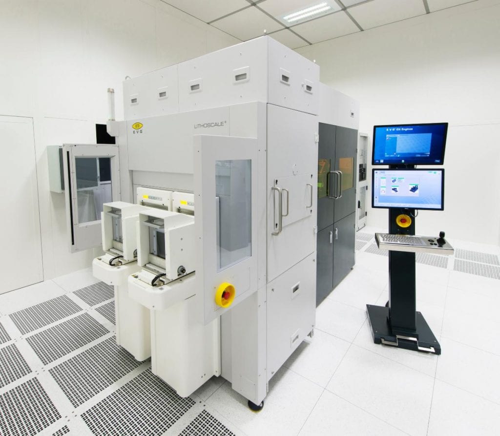
EV Group (EVG), a leading supplier of wafer bonding and lithography equipment for the MEMS, nanotechnology, and semiconductor markets, today introduced the LITHOSCALE® maskless exposure system — the first product platform to feature EVG’s revolutionary MLE™ (Maskless Exposure) technology. LITHOSCALE was developed by EVG to address lithography needs for markets and applications requiring a high degree of flexibility or product variation, including advanced packaging, MEMS, biomedical and IC substrate manufacturing. LITHOSCALE combines high resolution with no exposure field limitations, powerful digital processing that enables real-time data transfer and immediate exposure, and a highly scalable design. The result is the world’s first maskless lithography system for high-volume manufacturing (HVM) with up to a 5X increase in throughput compared to existing maskless exposure systems in the market. EVG has already received multiple orders for LITHOSCALE and will begin shipping systems to customers later this year.
Company executives will be available to discuss LITHOSCALE at SEMICON Taiwan, taking place this week at the Taipei Nangang Exhibition Center, Hall 1 (TaiNEX 1) from September 23-25.

New Requirements for Lithography
3D integration and heterogeneous integration are increasingly critical to enabling continuous improvements in semiconductor device performance. This had led to an increase in package complexity as well as in the number of package options available — driving the need for greater design flexibility and the ability to adopt both die- and wafer-level designs simultaneously in back-end lithography. MEMS manufacturing also poses challenges for lithography due to its complex product mix, which drives up mask/reticle overhead costs. In the IC substrate and biomedical markets, demand is growing for a higher degree of patterning flexibility to address a wide range of feature and substrate sizes. Rapid prototyping is also becoming more important in biotech applications, driving the need for more flexible, scalable and “ready-to-go” lithography approaches.
Traditional mask-based lithography solutions are not practical for many of these applications, especially those requiring fast prototyping and testing of new product designs or highly customized solutions, where the cost and time needed for producing, testing and reworking a large volume of mask sets can quickly add up. Additionally, for advanced packaging, existing back-end lithography systems face difficulties with nonlinear, high-order substrate distortions and die-shift-related issues, especially after die reconstitution on the wafer in fan-out wafer-level packaging (FOWLP). At the same time, existing maskless lithography approaches do not offer the combination of speed, resolution and ease of use necessary for HVM environments.
LITHOSCALE tackles the demand for design flexibility, high scalability and productivity, as well as low cost of ownership. Its mask-free approach eliminates mask-related consumables, while the tunable solid-state laser exposure source is designed for high redundancy and long life-time stability with virtually no maintenance and no re-calibration required. Powerful digital processing enables real-time data transfer and immediate exposure — avoiding hours of setup time for each digital mask layout as needed by other maskless lithography systems. The system is capable of individual die processing, while fast full-field positioning and dynamic alignment enable high scalability for a range of substrate sizes and shapes. The result is a highly versatile maskless lithography platform geared for a variety of micro-electronic production applications.
“LITHOSCALE is a major achievement for EVG and firmly establishes our technical leadership in lithography while opening the door to a new world of opportunities for digital lithography,” stated Paul Lindner, executive technology director at EV Group. “LITHOSCALE has been designed from the ground up to be a highly flexible and scalable platform, which enables high-volume device manufacturers to finally realize the benefits of digital lithography. Demonstrations with our customers and partners have shown that the applications that can benefit from LITHOSCALE are wide ranging and growing by the day.”