
EV Group (EVG), a provider of innovative process solutions and expertise serving leading-edge and future semiconductor designs and chip integration schemes, today announced that new developments in heterogeneous integration enabled by its wafer-to-wafer and die-to-wafer hybrid bonding, maskless lithography, metrology and infrared (IR) laser release solutions will be highlighted in multiple papers being presented later this month at the 2025 IEEE 75th Electronic Components and Technology Conference (ECTC), to be held May 27-30 in Dallas, Texas.
Hybrid Bonding Leadership
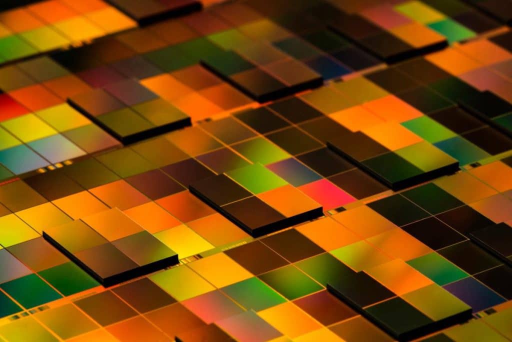
As the market and technology leader in wafer bonding, EVG provides the most complete portfolio of wafer bonding solutions, including hybrid bonding. The adoption of newer packaging technologies with tighter pitch requirements to support higher bandwidth needs for high-performance computing and AI applications are in turn fueling the need for new and different hybrid bonding techniques. According to TechInsights, the hybrid bonding market is expected to grow from US$26 billion in revenues in 2024 to US$112 billion by 2029, representing a compound annual growth rate (CAGR) of 28 percent—significantly outpacing the 7 percent CAGR forecast for the overall semiconductor market.
EVG is participating with the following professional development course, papers and posters in the ECTC technical program this year:
- “Wafer-to-Wafer and Die-to-Wafer Hybrid Bonding for Advanced Interconnects” (Professional Development Course – Tue., May 27, 8:00am – 12:00pm) – Dr. Viorel Dragoi, Chief Scientist for Wafer Bonding, EV Group
- “Integration, Materials and Equipment Innovations to Enable 100 nm Pitch W2W Bonding for Memory-to-Logic and Logic-to-Logic 3D Stacking” (Session 14, New Materials and Processes in Wafer-to-Wafer Hybrid Bonding – Thu., May 29, 9:30am) – co-authored with Applied Materials
- “Advanced FO PLP Digital Lithography Patterning Development for AI Devices” (Session 21, Meeting AI Challenges: Large Package Solution and Warpage Management for Advanced Packaging – Thu., May 29, 2:40pm) – co-authored with Fujifilm Electronic Materials
- “IR Laser Debonding for Silicon Based Temporary Carrier Systems Enabling 2.5D and 3D Chiplet Integration Processes” (Session 39: Interactive Presentations 3 – Thu., May 29, 10:00am – 12:00pm) – co-authored with imec
- “Process Approaches to Enable 200°C Hybrid Bonding With SiCN Bond Layer and 0.5 µm Pitch” (Session 39: Interactive Presentations 3 – Thu., May 29, 10:00am – 12:00pm) – co-authored with Applied Materials
- “Wafer-to-Wafer Bonding With Saddle-Shaped Wafers” (Session 40: Interactive Presentations 4 – Thu., May 29, 2:30 – 4:30pm) – co-authored with imec
EVG Heterogeneous Integration Solutions
EVG’s wafer bonding, lithography and metrology solutions enable the development and high-volume manufacturing of technology innovations in advanced packaging—including backside illuminated CMOS image sensors and other 3D-IC stacked devices—as well as in MEMS and compound semiconductors. Examples of EVG’s technology leadership in heterogeneous integration and wafer-level packaging include: breakthroughs in hybrid bonding to address the needs for 3D device integration; wafer bond alignment technology to address future 3D-IC packaging requirements; IR laser release technology to eliminate glass substrates for advanced packaging and enable thin-layer 3D stacking; maskless exposure for Fan-out wafer level packaging (FOWLP); and nanoimprint lithography (NIL) to support wafer-level optics (WLO) and photonic integrated circuits (PIC) manufacturing.
EVG also engages with companies and research groups across the technology supply chain to develop high-volume manufacturing solutions that drive new innovations in semiconductors, sensors and photonics for a wide variety of automotive, medical, industrial and home entertainment applications.