Final electrical test remains one of the best ways to assess a circuit’s ultimate viability. But we know, unfortunately, that even 100% end-of- line electrical testing of semiconductor wafers will not guarantee that chips will not fail in the field. Certain non-killer but marginal wafer defects can still slip through electrical testing if they have sufficient electrical connectivity, even though it may be less than optimal. And over the longer term, chips like these can become reliability “time-bombs.” In the end products, repeated thermal and electrical overstress can cause electromigration and push such circuits into failure.
Fortunately, there’s another tool that can catch many of these latent defects. It’s a way that can provide additional defect information, earlier in the process — using high-speed in-line macro defect inspection.
Good die may not all be equally good
Figure 1 is an in-line semiconductor macro wafer inspection picture showing a common surface scratch – in a “Z” shape – on a wafer. Now compare that with Figure 2, which shows the final electrical test result for the same wafer. You will notice that not all the die within the Z area failed. The elec- trical test seems to indicate that there are still a number of “good” (green) die within the Z pattern — even though we might reasonably suspect that additional die within that area could actually have been adversely affected by the scratch.

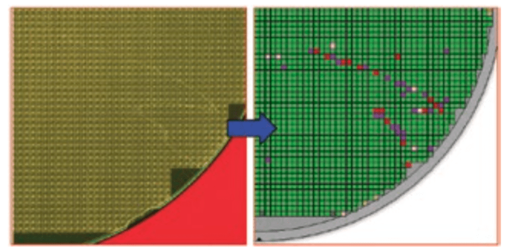
Figure 2. (R) The final electrical test result for the wafer shown in Fig. 1. Note that not all the die within the Z area failed
In Figures 3 and 4 we can see another example: Figure 3, from in-line semiconductor macro wafer inspection, clearly reveals a problem of inadequate photoresist coverage at the edge of the wafer. However, final electrical testing of the same wafer, shown in Figure 4, again reports fewer failed (non-green) die than might have been expected, given the extent of the photoresist issue.

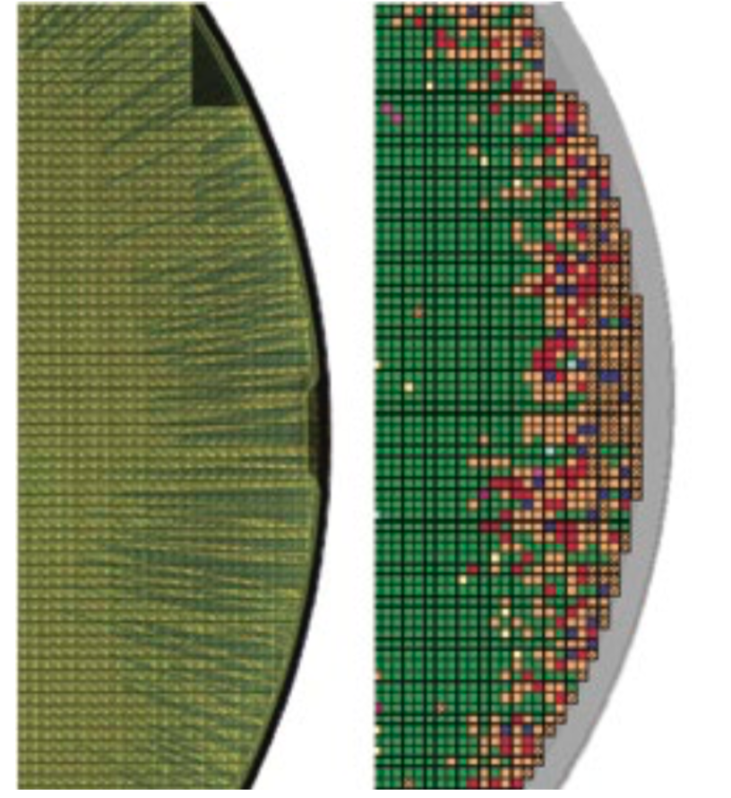
Figure 4. (R) Final electrical testing of the wafer shown in Figure 3 again reports fewer failed (non-green) die than might have been expected, given the extent of the photoresist issue.
So, as before, we might well suspect that at least some of those “good” die at the periphery of the failed areas may actually be compromised, at least to some degree.
More complete wafer defect information = improved yields and better inspections
Those are just two of the many “gray area” scenarios that allow marginal devices to get past electrical test and into customers’
hands. In the examples shown above, final electrical testing did not have the benefit of the earlier macro wafer inspection information. Fortunately, however, today’s ultra high-speed automated macro defect wafer inspection systems can automatically provide a wealth of additional defect data – to inform and improve every subsequent processing step and inspection.
Ultra-fast full-wafer macro defect inspection – to complement microsampling
Because of their ultra-high speed, today’s macro defect inspection systems have become an essential complement to micro inspection. For example, the EagleView from Microtronic can provide fabs with full-wafer semiconductor macro inspection of all the wafers in the lot, without recipes – in just a few minutes! So there’s no need for macro sampling.
This allows macro defect inspection to be used after many more process steps, to catch more problems earlier. Which means that fabs can take more specific corrective actions much sooner – to minimize scrap, increase yields, and reduce costs.