By Dick James
The International Solid-State Circuits Conference was held virtually last month from February 13th – 22nd, 205 papers in 35 sessions, with industrial participation from Analog Devices, Broadcom, Huawei Technologies, IBM, Intel, Qualcomm, Realtek Semiconductor, Renesas, Samsung, Sony, SK Hynix, STMicroelectronics, TSMC, Texas Instruments, and more.
Gate-All-Around (GAA, otherwise known as nanowire or nanosheet) transistors have been showing up in quantity in more process-related conferences such as IEDM and the VLSI symposia, but rarely if at all at ISSCC. In a sign that they are becoming mainstream, TSMC chairman Mark Liu showed off GAA-SRAM results in his opening keynote [1], and Samsung gave a conference paper on the same topic [2].
GAAFETs have inherently better channel control than finFETs, since the gate is wrapped around all the channel surfaces. FinFETs have improved performance over planar FETs, but they have the disadvantage that the gate width is quantized to the gate wrap-over distance on the fin.
One could argue that a GAAFET gate width is quantized to the gate wrap-around on the nanosheet and is dependent on the number of sheets; but it is easier to adjust sheet width than it is to alter fin height within a design, giving more flexibility.
TSMC
The TSMC data [1] was first shown at the TSMC Technology Symposium last August, and it has appeared a couple of times since, though I cannot find a conference reference for it.

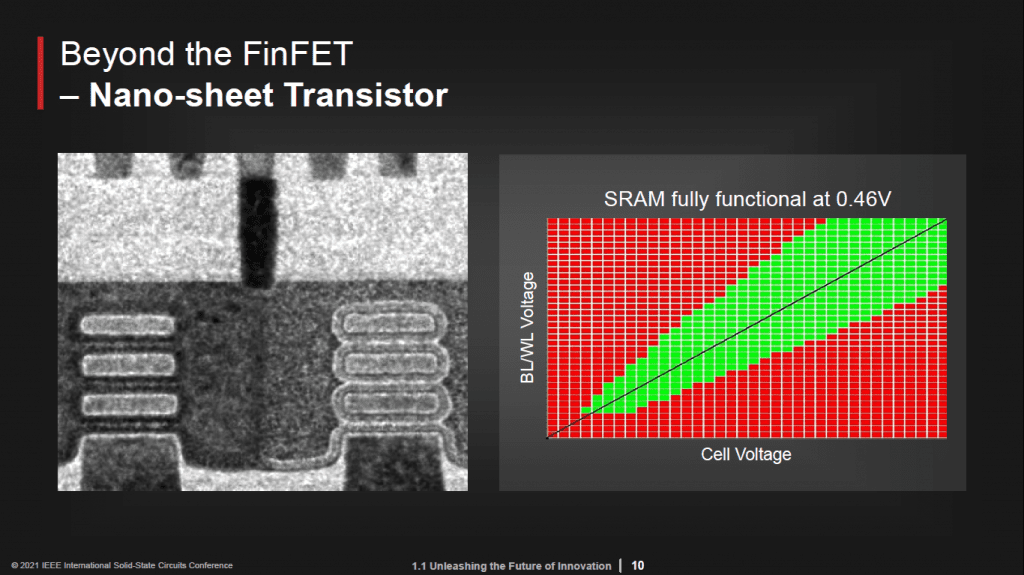
Mark Liu said:
“This nanosheet transistor achieved smaller drain-induced barrier lowering and sub-threshold swing to boost circuit performance as compared to previous technology generations. Transistor performance improvement translates directly into lower Vdd operation of SRAM. The shmoo plot shows fully functional SRAM at 0.46 V.”
At the Symposium it was stated that the data were from a 32 MB SRAM, though no other technical details were given. However, if we take the wild guess that the M0 pitch shown is 28 nm as in the 5N process, then the nanosheets are ~35 nm wide and ~6 nm thick. That gives us a channel width of 240 – 250 nm, or the equivalent of a 2+-fin transistor at current fin heights.
If the parallel with the 5N technology continues, CPP will be ~51 nm. We can also see that we have PMOS and NMOS transistors and contact on active gate has been used.
Samsung
In Session 24 of the conference Samsung presented “3nm Gate-All-Around SRAM Featuring an Adaptive Dual-BL and Adaptive Cell-Power Assist Circuit“. They seem to have gone with the acronymic flow in the business and changed their nomenclature from MBCFET (Multi-Bridge Channel FET) to GAAFET.
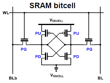
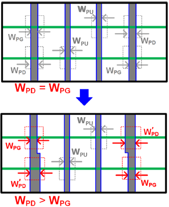
Samsung takes advantage of the ability to adjust nanosheet width to tune the SRAM bitcell transistors to improve performance margins, an option not available with a finFET cell. In a six-transistor bitcell we have three types of transistor, pass-gate (PG), pull-up (PU), and pull-down (PD):

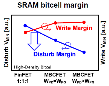
In a finFET, the PU:PG:PD gate width ratio is inevitably set to 1:1:1 for a high-density bitcell, while in their GAA-SRAM Samsung tried a different WPD:WPG ratio in the same footprint:

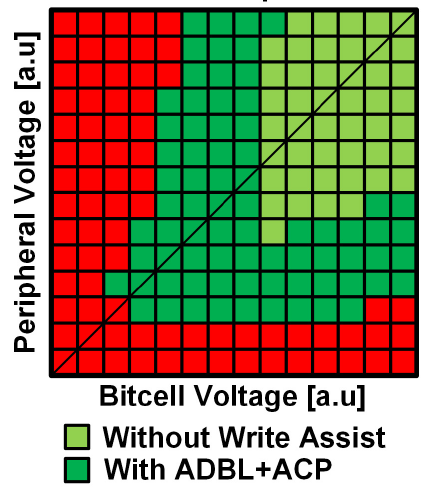
This improved the disturb margin quite noticeably, and even gave a slight improvement in the write margin:

Write margin is dependent on RVDDC (bitcell power-line resistance), RBL (bitcell bitline resistance), RPU (PU transistor on-resistance), and RPG (PG transistor on-resistance); RPU and RPG are already fixed by cell layout, so higher-level design was used to increase margin.
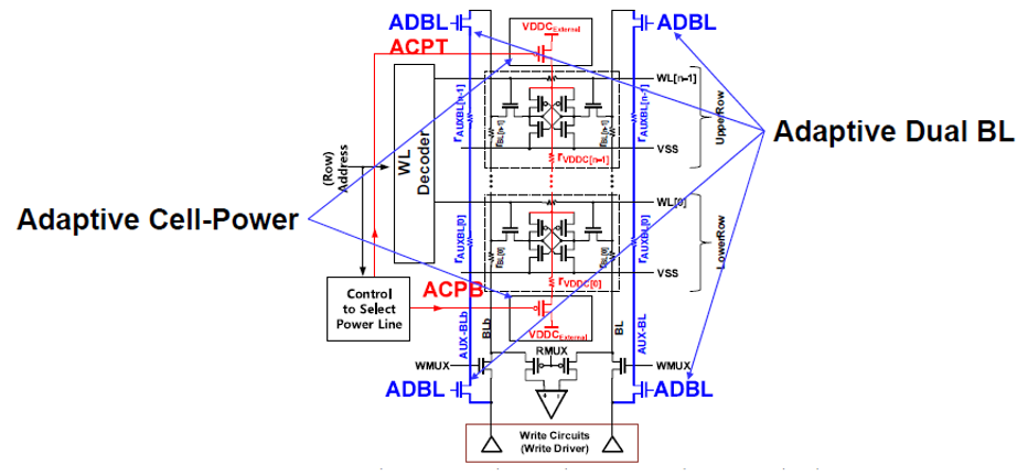
RBL was reduced by adding an Adaptive Dual-Bitline (ADBL) – essentially adding a second switchable bitline in parallel to the original bitline:

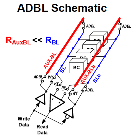
ADBL is ON for write, and OFF for read:

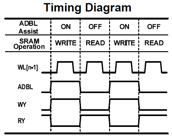
With ADBL ON, RBL is reduced by 70%; in read, with ADBL OFF, RBL goes back to normal, and CBL is not affected by CAUX-BL, so read margin stays the same.
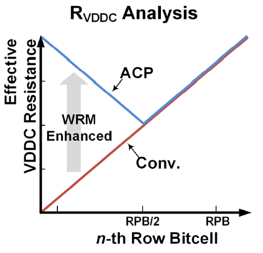
Write margin is also improved by raising RVDDC, so “Adaptive Cell-Power” (ACP) is used to increase it selectively. RVDDC for each cell is different depending on its position in the array, so ACP uses two power-switches at the bottom and top of the array, which is selectively switched dependent on the address. When a lower bitcell is activated, the upper switch is selected, and vice versa. Since power is supplied by the switch furthest away, and thus has a larger RVDDC, the write margin increases. In read, both switches are closed.

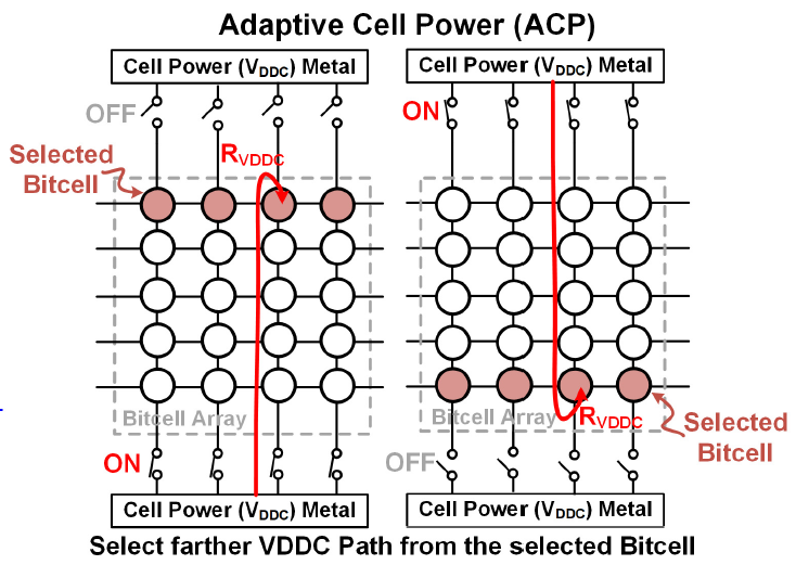
As you would expect, with this scheme, RVDDC reaches a minimum in the middle of the array, but overall the write margin is improved, compared with a conventional single power switch:

If we take ADBL and ACP into the design, we get this macro view:

And without knowing the starting VMIN, the cumulative VMIN reduction is up to 230 mV:

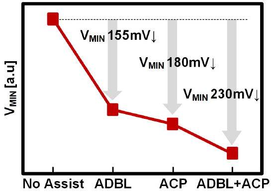
With a corresponding improvement in the Shmoo plot:

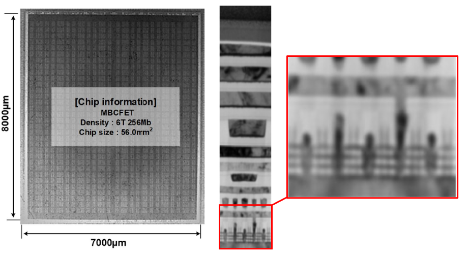
The GAA-SRAM was implemented in a 6T-cell, 56 mm2, 256-Mb test chip, and to finish the presentation we were shown a die photo and a TEM cross-section in the plane of the nanosheets. All the images are fuzzy, but we can see that there are at least ten copper metallization layers, and a stack of three nanosheets, similar to the TSMC device.

There have been numerous publications on GAAFETs from collaborative institutes such as imec and SUNY Albany, but now we are seeing more focused work from the foundries, and GAAFETs are on the roadmaps at 3 nm (Samsung), 2 nm (TSMC), and no doubt at Intel (5 nm?).
References
- M. Liu, “Unleashing the Future of Innovation” ISSCC 2021, paper 1.1, pp. 9 – 12
- T. Song et al., “3nm Gate-All-Around SRAM Featuring an Adaptive Dual-BL and Adaptive Cell-Power Assist Circuit“, ISSCC 2021, paper 24.3, pp. 338 – 340