In previous bulletins, we discussed the problem of partially-defective, marginal die that are still functional enough to pass final electrical test. Some of these “walking wounded” chips get past final testing, but in the customer’s end product, under ongoing stress, they may fail. This is a particularly serious issue with automotive, medical and other customers who demand maximum long-term device reliability.
The semiconductor industry has long used a process known as digital guardbanding to ink-off suspect die. This updates the die coordinates on the wafer map preventing shipment of suspect die. Guardbanding removes marginal die and also takes out additional die around the edges of clearly identified defective die, this added insurance is known as a “buffer.”
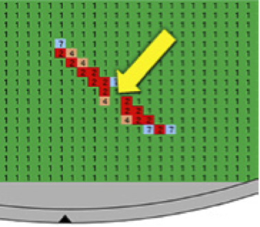
To accomplish this, neighboring-die algorithms may be used to automatically search wafer maps and apply guardbanding based upon proximity to known bad die. For example, in Figure 1, guardbanding might have been used to remove the questionable “good” area (indicated by arrow) within the scratch zone.

Putting guardbanding to work earlier
To date, guardbanding has been used primarily at end-of-line testing — but it can also play a critical role during in-line inspection. That’s because final inspections can still miss a variety of defects that occur earlier inline. For example, certain in-line problems can get covered over by subsequent processing steps and become very difficult to detect later. For this reason, in-line macro defect inspection and in-line guardbanding have become essential complements to traditional micro inspections and electrical testing.

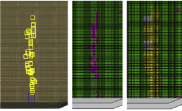
Figure 2c. Wafer probe with guardbanding.
In-line macro defect inspection and guardbanding — at high speed
With today’s generation of ultra-high speed automated macro inspection tools, such as the EagleView from Microtronic, fabs can now inspect every wafer in the lot — without need for sampling or recipes. This allows fabs to in- spect many more wafers at manymore processing steps — to correct process and equipment issues sooner, and to save more wafers from being scrapped or affected in an excursion. And in addition to identifying in-line macro defects, EagleView also makes it easier to guardband those defects…

Some fabs still use a hand-drawn paper tracing system to enable guardbanding, which is time consuming and inaccurate. With the EagleView platform, guardbanding is performed directly on a high-resolution wafer image, for maximum precision and ease.
The tool may be set to automatically add guardbanding to some defects, or an operator may add guardbanding selectively to specific defects. Some types of scratches, for example, may scatter particles onto surrounding die. Figure 2a shows a scratch detected by macro inspection. Figure 2b shows the same wafer at wafer probe, and Figure 2c shows the scratch with guardbanding added.
Integrating defect data from more sources
The macro inspection tool produces a true high-resolution, permanent-record image of every wafer, which builds a powerful, comprehensive database of defect information for the fab (Figure 3). These files provide a rich and valuable data resource for end-of-line testing, for root cause analysis of current in-line problems or to refer to at any time in the future. Importantly, the EagleView system can also import KLARF files from micro-inspection tools (Figure 4a) and overlay them onto the EagleView image (Figure 4b) where a user-defined buffer can be applied real-time. The wafer probe map is displayed in Figure 4c, and Figure 4d shows the resulting guardbanded wafer probe map. EagleView can use SEMI standard G85 wafer maps or apply a translator for legacy probe map systems.

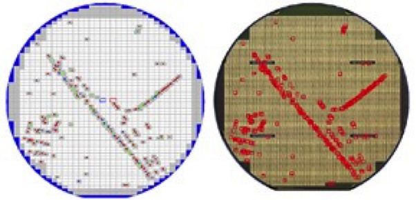
Figure 4b. KLARF file overlaying EagleView wafer image.

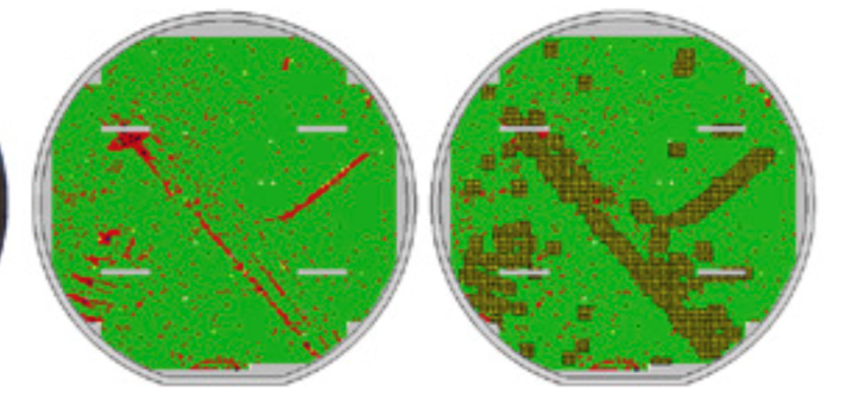
Figure 4d. Wafer probe map with guardbanding.
Doing more to enhance chip quality
Today, there are still many ways for defects to slip through final testing and get shipped to customers. However, in-line macro defect inspection and guardbanding are important and powerful tools that can help fabs to catch more problems earlier — to improve chip reliability, reduce returns and keep customers happier.
to customers. However, in-line macro defect inspection and guardbanding are important and powerful tools that can help fabs to catch more problems earlier — to improve chip re- liability, reduce returns and keep customers happier.