By Dick James
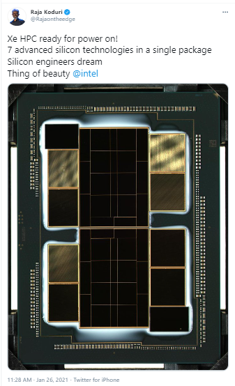
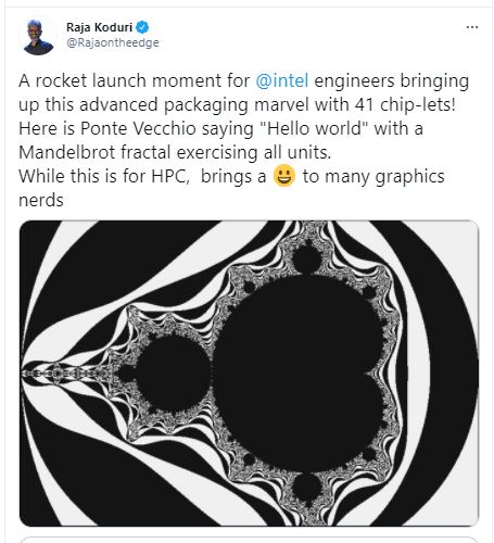
Occasionally, we will see something in the media that we think worth commenting on, and post as an “In Case You Missed It” (ICYMI) blog. In this case, it was a Jan 26 Twitter post by Intel’s Raja Koduri (@rajaonthe edge), showing a complex multi-die part that appears to be the Ponte Vecchio high-end GPU, announced by Raja in his keynote at the Intel HPC Developer Conference just before SuperComputing 2019.

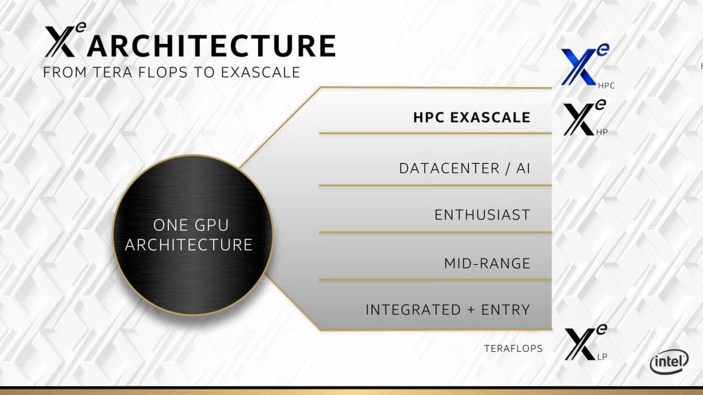
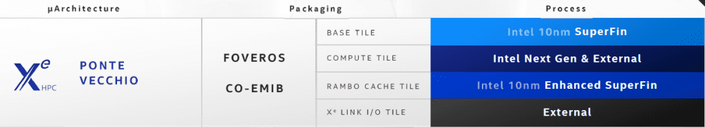
Intel’s Xe GPU architecture replaces the previous “Gen” (Gen 1 – Gen 11) architecture; Gen 11 is in the Ice Lake processors currently on the market. Xe apparently means ‘eXascale for Everyone’, and ranges from Xe-LP (Low-Power) to Xe-HPC (High Performance Computing):

Ponte Vecchio (PVC) is the Xe-HPC entry into Intel’s GPU spectrum. As you can see, it is a complex piece of technology:

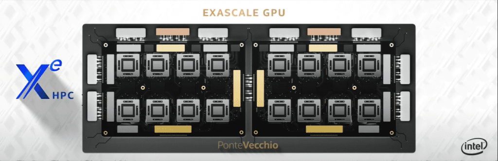
PVC is split into two segments, with eight compute tiles in each, and four “Rambo” cache memory chips between the two rows of compute tiles. Also identified during the talk were two HBM memory stacks at the extreme left and right ends of the schematic, and elsewhere are Xe-link I/O tiles. The Rambo chips are not clear in the image above, so here is another illustration:

PVC was claimed to use Foveros stacking for the compute dies, and EMIB links for the HBM memory – and the first use of the 7-nm process:
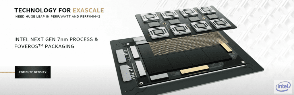
At last year’s Architecture Day, a little more detail was given of what parts come from where:


From this it appears that the compute tiles are either Intel 7-nm, or could be out-sourced to a foundry, and the I/O dies certainly are. The base die has evolved from the 22FFL process used for the Lakefield base die to the 10SF process, so presumably has quite a bit more processing potential.
If we look at the photo posted by Raja, the layout has changed quite a bit, and the dies are packed very tightly.
We can see two assemblies, each with a total of twenty dies (presumably on a base die), and five dies surrounding each assembly. Given the foregoing information, it seems likely that the twenty dies are Foveros-stacked on a base die, and the surrounding chips are connected by EMIB, as are the two assemblies. This was shown schematically at last years Architecture Day:
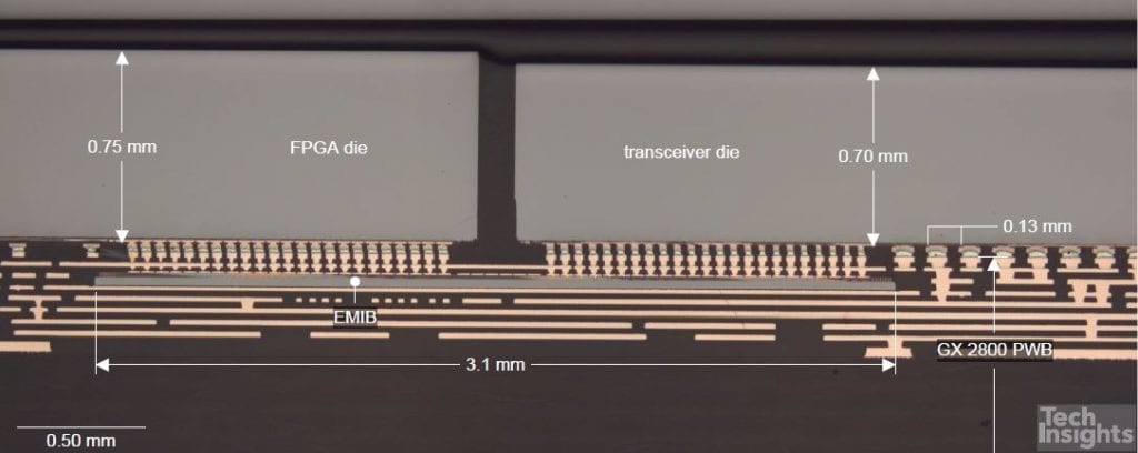
We have seen EMIB before, in a Stratix-10 FPGA:

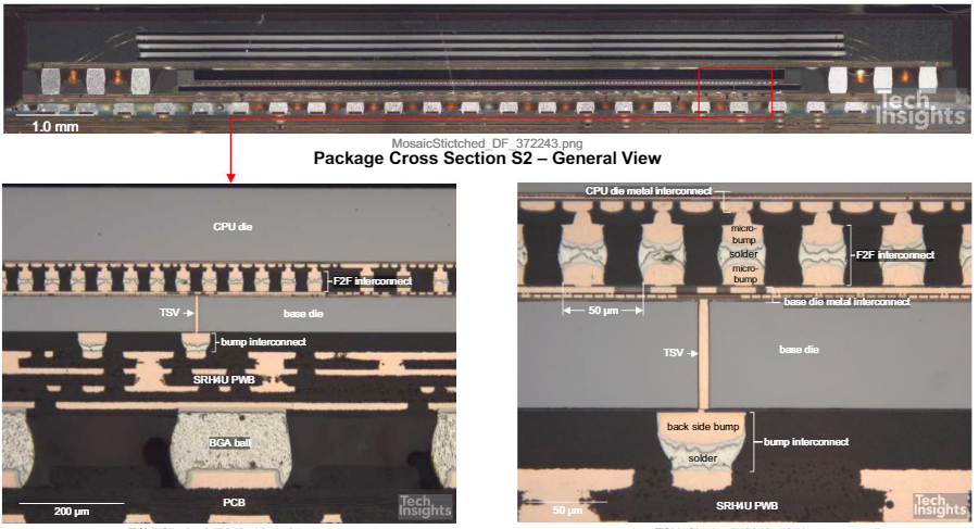
And Foveros, in the Lakefield processor:

Ponte Vecchio does not have the package-on-package DRAM as in the Lakefield, and the base die (or dies?) are likely more complex since 10SF has 16 metal layers versus 22FFL’s ten.
There has been a fair bit of media speculation as to what the various dies are on the package, but Usman Pirzada of Wccftech drew on their sources to try and identify them and claims to have the dies identified shown here:

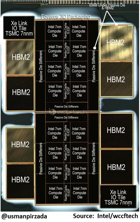
The same as the schematic above, there are eight compute dies on the base die in each segment, with the Rambo cache in the centre, and HBM2 memories on both sides. Each compute tile is reported to contain 128 execution units (EUs) each for a total of 1024 EUs and 8192 cores. The additional chips are Xe Link I/O dies in opposing corners, and eight dummy dies per segment on the base die. The dummies are presumably there to add stiffness and stability to reduce stress on the lower die – that also implies to me that it has been thinned substantially, possibly to aid heat dissipation. (The Lakefield base die was thinned to ~80 µm.) They take up almost 40% of the area, so one assumes that their presence is critical.
Strangely, the HBM2 parts have two different die sizes, maybe reflecting dual sourcing. The more-square HBM2s on the top right and bottom left of the package actually have the same aspect ratio as the 16-GB Samsung Flashbolt HBM2, so it is tempting to think that has been used. In that case it looks as though there is 64 GB DRAM available.
Raja teased us that there are seven advanced technologies in a single package – here are my guesses:
- Xe architecture
- Intel 7nm
- Intel 10SF
- TSMC 7nm
- Foveros 3D Packaging
- Rambo cache
- 16 GB HBM2
I was curious about all the die sizes, but lacking a scale bar, and unable to find any die size information for the Flashbolt to use as a reference, I have taken a guess that the passives on the organic substrate are a standard spacing and the same as in other Intel products. Using those to give me some scale, I have come up with the following die sizes:
| Base die | ~529 mm2 (~19 x 27 mm) |
| Compute tile | ~34 mm2 (~5.5 x 6.2 mm) |
| Rambo cache | ~12 mm2 (~2 x 6 mm) |
| Side dummy die | ~27 mm2 (~3 x 9 mm) |
| Bottom dummy die | ~18 mm2 (~6 x 3 mm) |
| Xe Link I/O die | ~65 mm2 (~9.7 x 6.7 mm) |
| Top left/bottom right HBM2 | ~89 mm2 (~8.5 x 10.5 mm) |
| Top right/bottom left HBM2 | ~102 mm2 (~9.7 x 10.5 mm) |
They are very much approximations, but the DRAM sizes don’t seem too outrageous for 16-Gb dies; they are larger than commodity DRAM, but then space has to be allowed for the TSV keep-out areas.
This is likely the first product image of the Co-EMIB technology and an Intel 7-nm die, and clearly this is a very impressive piece of engineering – and hopefully it powers on successfully. Ponte Vecchio is a critical part of Argonne National Lab’s Aurora Exascale supercomputer, so Intel still has serious challenges in ramping up both 7-nm and Co-EMIB to meet the needs of the system and others in the future.
Postscript
It appears that Ponte Vecchio has powered up successfully – on Feb 6 Raja posted a follow-up tweet:

This business never slows down!