By Dick James, Contributing Editor
Samsung gives a second paper this session, detailing (2.5) A Novel Integration of STT-MRAM for On-chip Hybrid Memory by Utilizing Non-Volatility Modulation, with Jeong-Heon Park as lead author. “We demonstrate a novel way of integrating STT-MRAM for on-chip hybrid memory which exhibits either features of high-retention or high-speed implemented in separate zones in a single chip. For satisfying high temperature retention requirement, tailored MTJs are shown to support >10-year retention at 220℃.” MRAM switching protocols can be tuned for either high speed or high retention, so here we have a process which gives the option of both on the same die.
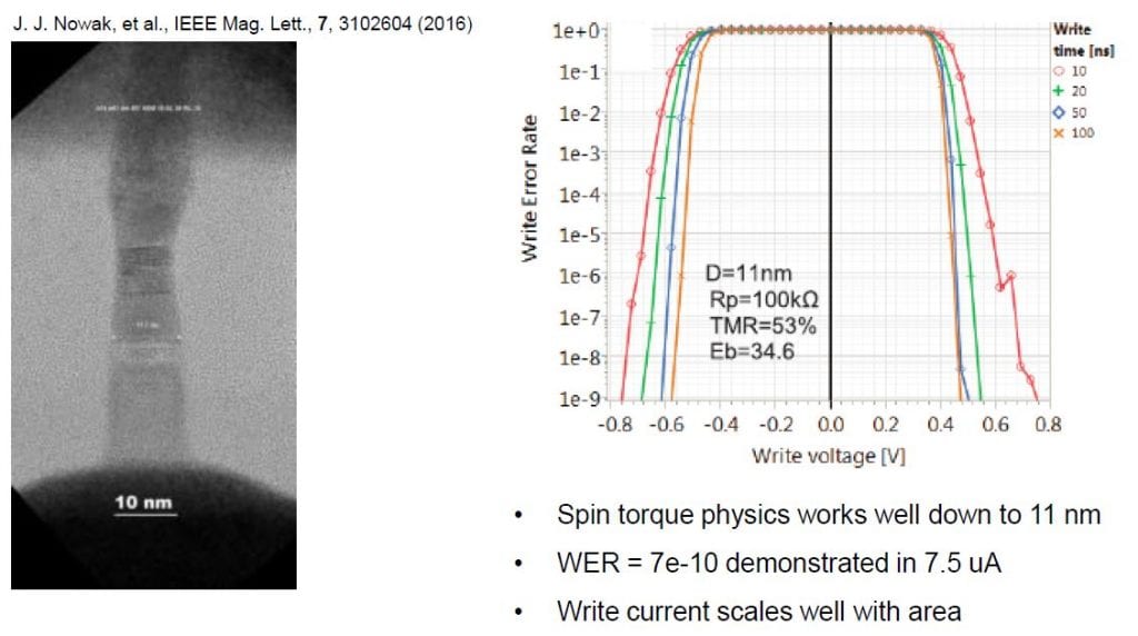
And even though IBM no longer has its own production fabs, it has a long history in MRAM research and that continues with Guohan Hu discussing Spin-transfer torque MRAM with Reliability 2ns Writing for Last Level Cache Applications (2.6). “Reliable 2ns switching of STT-MRAM devices was achieved for the first time by demonstrating 100% write-error-rate yield at 1e-6 write-error floor of 254 devices. A single device with less than 1e-11 write error rate was demonstrated with 2ns write pulses. Reliable 3ns switching was demonstrated with a completely different stack design.”
IBM has been steadily pushing the limits of MRAM, and have demonstrated MTJ sizes down to 11 nm, steadily pushing the limits of MRAM, and have demonstrated MTJ sizes down to 11 nm, and switching speeds of 10 ns [5]. In this presentation it seems we are now down to 2 ns.

TSMC is recognizing the need for embedded MRAM that can take the automotive environment of potentially higher temperatures and magnetic fields in 2.7, 22nm STT-MRAM for Reflow and Automotive Uses with High Yield, Reliability, and Magnetic Immunity and with Performance and Shielding Options, William Gallagher et. al, TSMC
“We demonstrate high yielding solder-reflow-capable STT-MRAM embedded in 22nm CMOS. The technology supports -40 to 150°C operation, retains data through six solder reflow cycles. and has ten-year native magnetic field immunity >1100 Oe at 25°C at 1ppm bit upset level, with a shield-in-package demonstrating even higher immunity. Trading off retention, higher performance and endurance are also demonstrated. The researchers say that by trading off some of the reflow capability and using smaller MTJs, even higher performance can be achieved (e.g., 6ns read times/30ns write times), making them appealing for artificial intelligence inference engines.”
TSMC has a range of 22-nm offerings based on its 28-nm HPC+ process; 22ULP, 22ULL, and 22ULL low Vdd. 22ULP is an optical shrink providing 10% area reduction with more than 30% speed gain or more than 30% power reduction. The 22ULL incorporates the MRAM and is quoted as having triple gate oxide and ULL SRAM.
They also presented at this year’s VLSI Symposia [6], giving initial results for the 22-nm MRAM implementation. The MTJ stacks are between metals 3 and 4.
The figures below (Figs. 10a & b) show (a) the normalized read window at 1ppm fail rate of a 4Mb array for a wafer repaired (by ECC) at 125°C; and (b) by-die bit upset rates after three and six solder-reflow cycles for bits initially in the low (Rp) or high (Rap) resistance states.

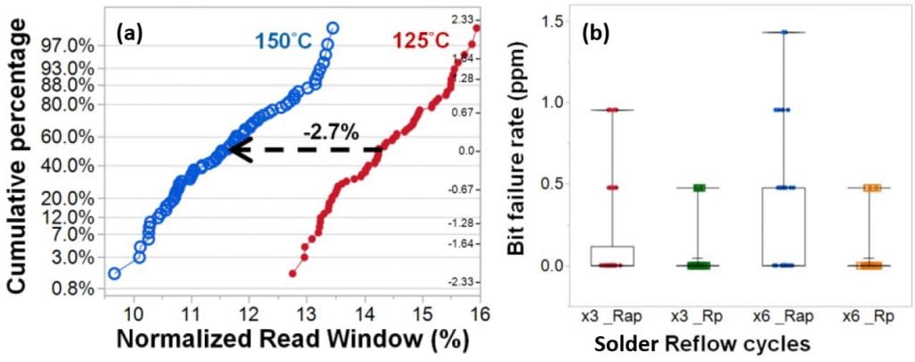
In (a) the 150°C read window is reduced, but is still enough for no loss of repaired die yield between 125°C and 150°C. In (b), the results indicate 10-year retention at >225°C [6], and failures are way below the 10ppm level allowed for reflow repair.
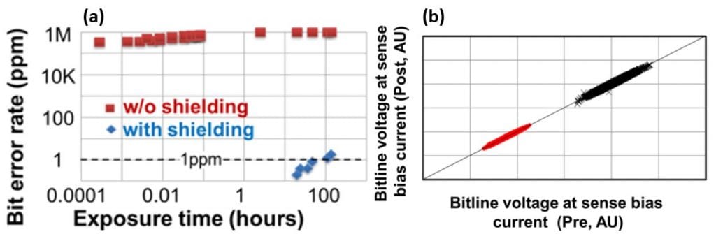
The plot below left (Fig. 11a) shows bit error rates for a 4-Mb sub-array with and without an in-package magnetic shield, exposed to a 3.5 kOe-field NdFeB magnet just above the packaged die for various times at 25°C. Unshielded bit failure rates sample are ~30% after ~1 second exposure; with the shield, they were below 1ppm for ~80 hours, a reduction >106in bit failure rate provided by the shielding.
Below right (Fig. 11b), we see bit stability before and after 108 write cycles at -40°C. Voltages for the parallel (colored) and anti-parallel (black) states are well separated and stable – no shift can be inferred.

The paper also includes results for smaller MTJs with higher performance, with high retention but not solder reflow capability.
While Monday afternoon has the above papers, there is also a poster session on the Wednesday morning in the Yosemite Room, and the 11th MRAM Global Innovation Forum on Thursday after IEDM is over, in the Imperial Ballroom from 8.45 – 5.30.