By Dick James, Contributing Editor
Session 2 (Memory Technology – STT-MRAM) on Monday afternoon at IEDM has a series of industrially-based papers, starting with Everspin, one of the few commercial producers of MRAM; Demonstration of a Reliable 1 Gb Standalone Spin-Transfer Torque MRAM For Industrial Applications, Sanjeev Aggarwal et. al, Everspin Technologies.
“We demonstrate reliable operation of our 1 Gb standalone STT-MRAM product over a temperature range of -40C to 110C. Well-behaved read and write distributions over 4 sigma enable an endurance lifetime of 2e11 cycles and data retention of 10 years at 85C.” The 1-Gb parts are made in 28-nm technology, likely at GLOBALFOUNDRIES’ Singapore fab.

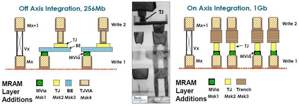
The device was detailed at the Flash Memory Summit back in August [1], and it appears that there is a structural change from the 256-Mb version; the MRAM stack is now on-axis with the write-1 and write-2 lines, as opposed to being offset in the earlier version. The TJ layer is the tunnel junction layer, more often referred to as the magnetic tunnel junction (MTJ).
In addition, the specifications have evolved from 1.5V DDR3 VDD/VDDQ, JEDEC DDR3 ball configuration to the 1.2V DDR4 VDD/VDDQ, DDR4 ball configuration. Looking at the schematic above, I’m curious to see if we will find out what is in the trench – some sort of extended metal stack?
Then we have a series of embedded MRAM talks, with Samsung up next, paper 2.2, 1 Gbit High Density Embedded STT-MRAM in 28nm FDSOI Technology, presented by Kilho Lee:
“High density 1Gb embedded STT-MRAM in 28nm FDSOI technology was successfully demonstrated. Based on the highly reliable and manufacturable eMRAM technology, high yield over 90% was achieved with satisfying read, write function and 10 years retention. Improved endurance up to 1E10 cycles was achieved to broaden eMRAM applications.”
Back in IEDM 2016 they had a paper “Highly Functional and Reliable 8Mb STT-MRAM Embedded in 28nm Logic” [2], fabbed in their 28nm LPP logic technology. Since the MTJ stack is integrated into the back-end metallization, the front end can be bulk silicon or FD-SOI, so I’m guessing that we could have some clues here to the upcoming talk.
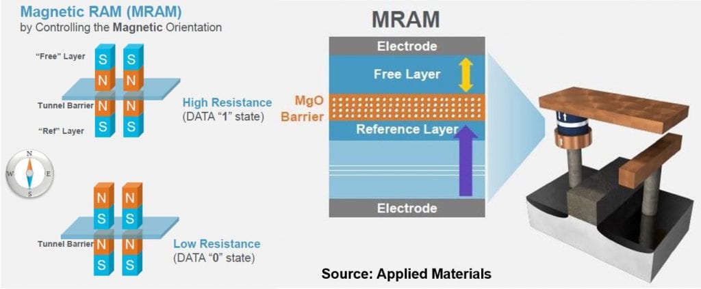
Data storage in the type of MTJ used here relies on the Perpendicular Magnetic Anisotropy (PMA) created by interfacial anisotropy between MgO and CoFeB layers. The magnetic state of the free CoFeB layer can be switched to be parallel (P) or anti-parallel (AP) to a reference layer; if it is parallel, we have low resistance (RP), if anti-parallel, higher resistance (RAP). Switching is done by forcing a current in one direction to go from P to AP, and in the reverse direction to go from AP to P.

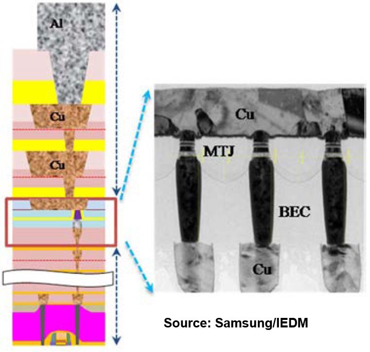
Samsung’s MRAM stack in the 2016 paper used MTJs with single MgO and CoFeB (CFB) layers. The MTJ is 38 – 45 nm in diameter, and the bottom electrode contact (BEC) is tungsten (and the top contact too, looking at the image).

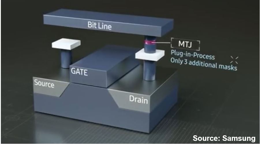
Last March Samsung announced the mass production of eMRAM in their 28FDS process, claiming a write speed ~1000 times faster than eflash, and of course lower voltages, since we don’t need to push charge through a dielectric layer. They also say that only three extra mask layers are needed:

In the press release they don’t discuss the product being shipped, but they do state that a 1-Gb test chip will be taped out, and presumably this talk will give us the details.
GLOBALFOUNDRIES has been promoting MRAM in their 22FDX process, so 2.3 considers a Manufacturable 22nm FD-SOI Embedded MRAM Technology for Industrial grade MCU and IOT Applications, by Vinayak Bharat Naik et al. “We demonstrate the manufacturable 22nm FD-SOI embedded-MRAM by achieving product functionality and reliability in package level at -40~125 °C. The product reliability is confirmed by passing LTOL, HTOL, 1M endurance and 5x-solder reflows tests. In addition, we demonstrate the macro capability to cover magnetic immunity of >500 Oe.”
They had a similarly titled paper at last year’s IEDM, 22-nm FD-SOI Embedded MRAM Technology for Low-Power Automotive-Grade-1 MCU Applications. That was subjected to similar testing regimes, including 1M endurance and 5x-solder reflow, pushed to -40~150 °C for the Auto-G1 rating. No details of the MTJ stack were given; maybe this year!
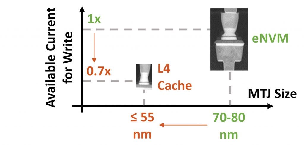
Intel has announced the integration of MRAM into their 22FFL technology [3], though it is not clear that the next talk 2.4, 2 MB Array-Level Demonstration of STT-MRAM Process and Performance Towards L4 Cache Applications (Juan G. Alzate et al., Intel Corporation), is actually based in the 22FFL process. Given that the MTJ (magnetic tunnel junction) size has been reduced from ~80 nm to ~55 nm (~70%), it is tempting to speculate that we have MRAM intended for the 1271 14-nm SoC process. In the figure below we can see the scaled (and improved) MTJ stack.

At last year’s IEDM [3] we were shown a schematic of the 22FFL MTJ stack (Fig.6):

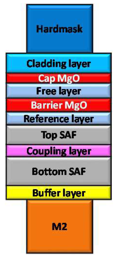
Intel has put the free CoFeB layer between two MgO interfaces, which enhances the anisotropy and hence data retention. The synthetic antiferromagnetic (SAF) layers improve the thermal stability and stabilize the magnetization of the reference layer [4].
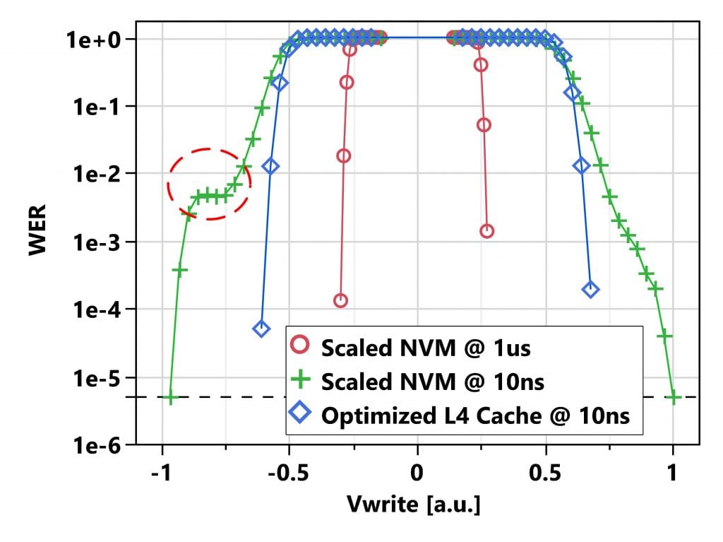
Scaling the MTJ reduces the write current, which sounds like a good idea, but that is related to the write time, and there is a trade-off for tunnel oxide wear-out between shorter pulse length/higher current, and longer pulse/lower current, putting boundaries of endurance vs write-error-rate (WER).
When optimizing the technology, Intel found a voltage “ballooning” phenomenon (in the dashed circular area in the figure below) that arose with write times of 10ns, but not with longer 1µs write times, which increased the WER for L4 cache beyond specification. This was eliminated by tuning the MTJ stack.

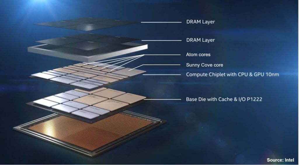
In this paper the MRAM MTJs are targeted as memory for L4 cache, which if I remember rightly, has been provided in the past by Intel’s e-DRAM. Given that this was actually on a separate die, that also raises the possibility that this could be in the base die of a Foveros stack:

Whatever the target process, Intel demonstrated 2 MB arrays of the scaled MTJs devices, “meeting L4 cache specifications across all proposed temperatures of operation. The technology achieves ECC-correctable bit fail rates for a 20 ns write time, a 4 ns read time, endurance of 10e12 cycles, and retention of 1 second at 110oC.”
Part 2 of this blog coming soon