Intel Has 13 Talks at the VLSI Symposia in June, Including Intel 4
Shannon Davis
The VLSI Symposia are coming up on June 12 – 17, at the Hilton Hawaiian Village in Honolulu, and recently their media associates released the tipsheet describing some of the upcoming papers.
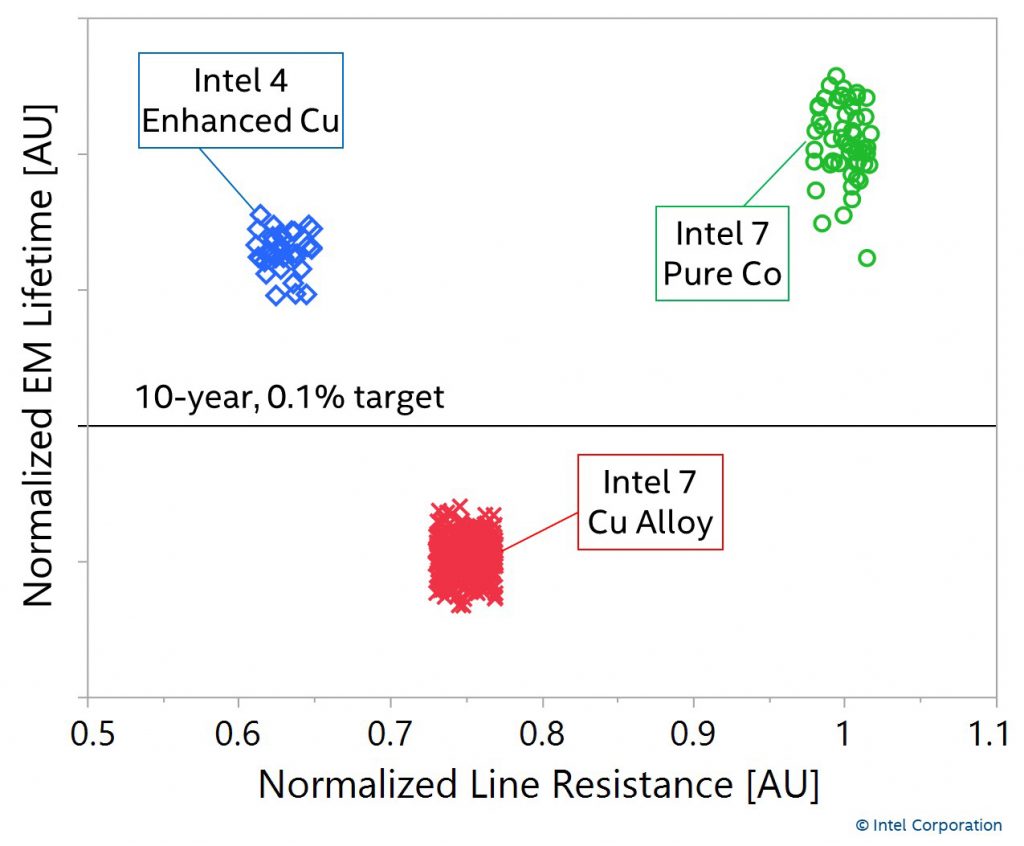
Contributed by Dick James, Fellow Emeritus, TechInsights The VLSI Symposia are coming up on June 12 – 17, at the Hilton Hawaiian Village in Honolulu, and recently their media associates released the tipsheet describing some of the upcoming papers. The detailed program is available here. Of the thirteen papers Intel is presenting at the conference, three are noted in the tipsheet. In the Advanced CMOS category, Intel are up first in the first session (T1-1), with “Intel 4 CMOS Technology Featuring Advanced FinFET Transistors Optimized for High Density and High-Performance Computing”. Intel 4 (formerly Intel 7-nm) claims 2X area scaling of the high-performance logic library over Intel 7 (formerly Intel 10ESF), and greater than 20% performance gain at iso-power. The scaled high-performance library uses 50 nm gate pitch, 30 nm fin pitch and 30 nm minimum metal pitch. That compares with 60 nm CPP, 34 nm fin pitch and 36 nm metal pitch for Intel 7 (source: TechInsights). It has eight VT levels (4 NVT + 4 PVT), spanning a range of 190mV for NMOS and 180mV for PMOS. As announced earlier, EUV lithography is used extensively to simplify the process flow and improve yield, including the lower metal layers. The interconnect stack features 16 metal layers with enhanced copper metallurgy at critical lower layers to deliver improved electromigration and lower line resistance.
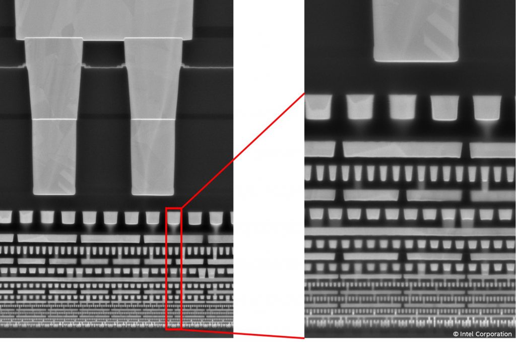
Cross-sectional view of the Intel 4 interconnect stack.
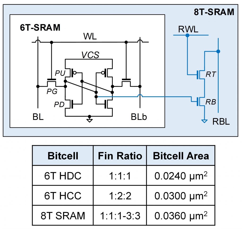
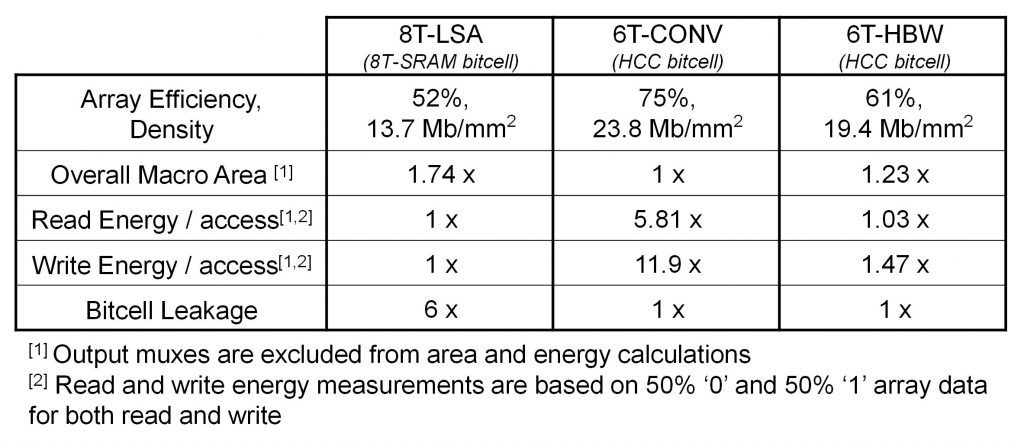
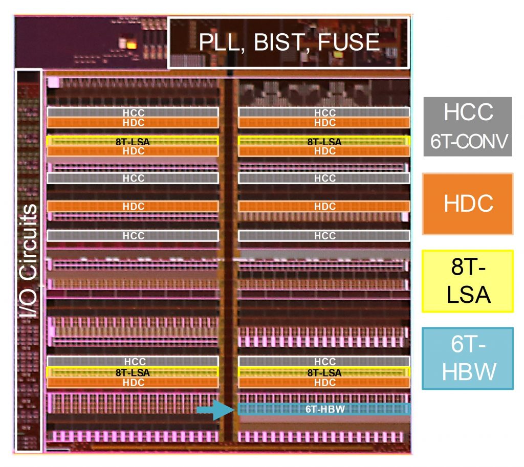
The following figure shows that the electromigration and line resistance properties of the updated copper are improved compared with both the Intel 7 copper and cobalt metallisation. Intel 4 SRAMs are discussed in paper C24-1 “Energy-Efficient High Bandwidth 6T SRAM Design on Intel 4 CMOS Technology”. An optimized 6T SRAM design at 0.03 μm2 bitcell area is presented, with a similar power to an 8T cell, and a 5.6x dynamic power reduction from the conventional 6T design. The bitcells are shown here: The minimum bitcell in Intel 7 is 0.367 μm2, so the high-density cell listed above is a 35% shrink. A 60 kB test macro was generated giving the following results:
Table 1: Comparison of density and energy per access for 60kB SRAM macro implementation.
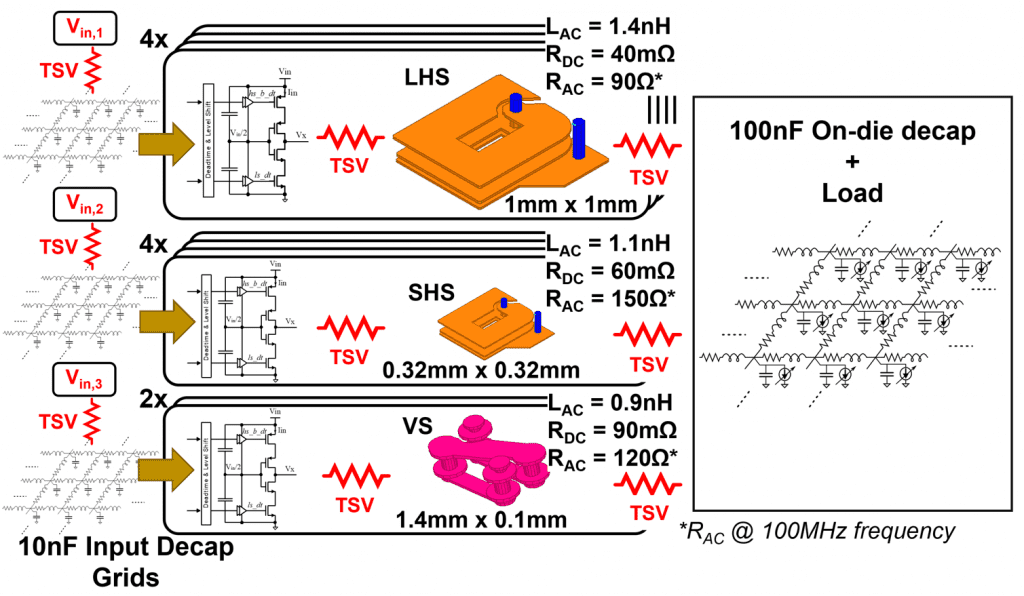
We are also shown a die shot of the test chip with the different SRAM blocks outlined: In the context of More-than Moore, Intel will report on their advanced system-in-package (SiP) power management, integrating heterogenous chiplets with their 3D-TSV-stacked SiP design on a 22nm active silicon interposer (paper C22-1, “Fully Integrated Voltage Regulators with Package-Embedded Inductors for Heterogeneous 3D-TSV-Stacked System-in-Package with 22nm CMOS Active Silicon Interposer Featuring Self-Trimmed, Digitally Controlled ON-Time Discontinuous Conduction Mode (DCM) Operation”). Different forms of inductors embedded in the package substrate are directly connected with 3D-TSVs to fully integrated voltage regulators (FIVRs) on the interposer die in a tiled form. The power efficiency is flat across a range of 10 mA – 300 mA for a single tile, and up to 1A range by selective ganging of regulators on neighboring tiles. The test setup is shown below.
Intel’s 10-tile fully integrated DCM-voltage regulator test setup with various TSV-based inductors for power/efficiency/area tradeoff.