By Dick James
Thanks to Covid-19, IEDM goes virtual this year, over the weeks of December 5 – 18th. After scanning through the advance program, and the tipsheet, a couple of papers from Intel caught my eye, one on complementary stacked nanoribbon transistors, and the other detailing embedded DRAM using anti-ferroelectric (AFE) capacitors.
Starting with the nanoribbon paper:
20.6 3-D Self-aligned Stacked NMOS-on-PMOS Nanoribbon Transistors for Continued Moore’s Law Scaling, Cheng-Ying Huang, et al.
There has been speculation that Intel’s 5-nm process will be their introduction of nanosheet/nanoribbon technology, but very few conference papers on the topic that I have seen have been published by Intel.
A year ago Jim Keller, formerly of Intel, gave a talk on Machine Learning, and presented this device evolution, and it seems likely that this is what we could see in upcoming generations:

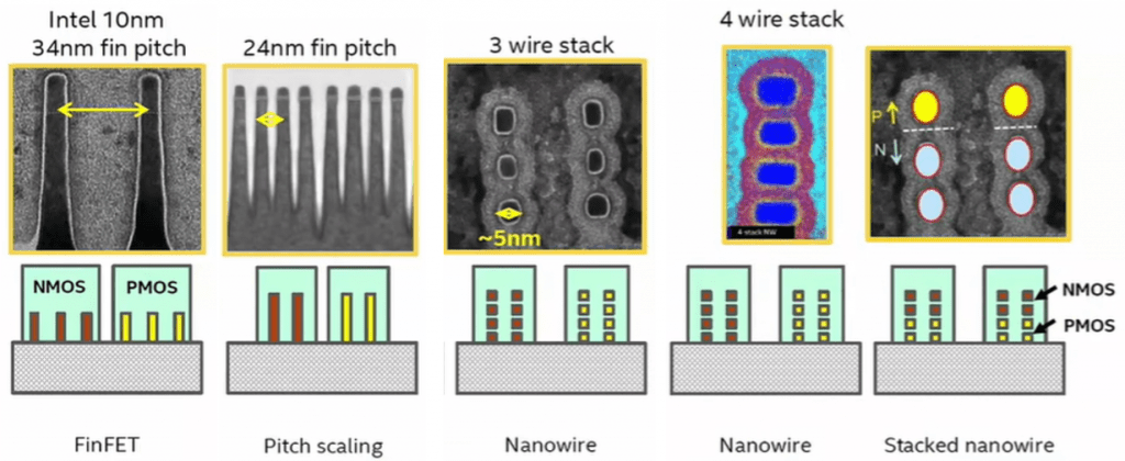
Looking at this, it’s tempting to think that the 7-nm node will have a 24-nm fin pitch, and the 5-nm will be the nanosheet (rather than nanowire) introduction. Paper 20.6 looks ahead to the stacked-nanoribbon phase:
“We demonstrate 3-D self-aligned stacked NMOS-on-PMOS multiple Si-nanoribbon transistors with successful integration of vertically-stacked dual source/drain and dual-metal-gate processes. Both NMOS and PMOS show high performance and superior short-channel control. A functional CMOS inverter is demonstrated with well-balanced voltage-transfer-characteristics. This novel transistor architecture is promising to continue Moore’s law scaling.”
A vertically stacked dual source/drain epitaxial process is used, together with dual metal gates, allowing P- and N-nanoribbons and Vt adjustments for both. This gives excellent electrostatics – subthreshold slope of <75 mV/decade, and DIBL of <30 mV/V for gates ≥30 nm. Below we have a schematic of the inverter on the left, and on the top right a TEM cross-section of the gate with the P-epi ribbon below, and a blob of N-epi above. Bottom right is a linear section of the gate showing the N- and P- ribbons embedded within it. Gate length is 40 nm, and we can see that nanoribbon width is 13 nm, and I guesstimate ~5 nm thick.

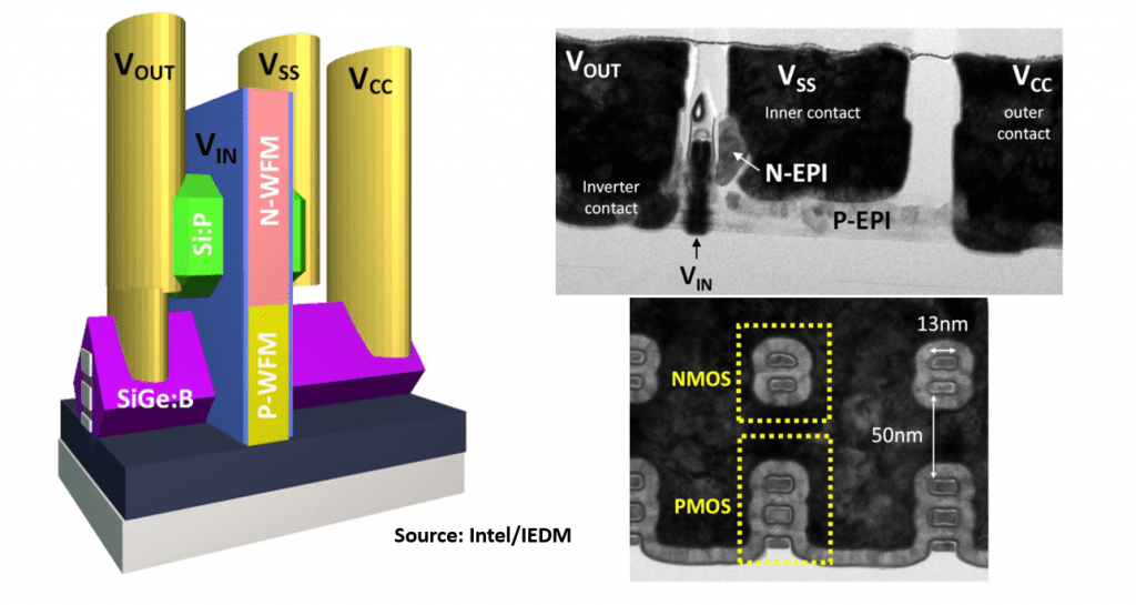
Fig. 2 Inverter schematic (left), TEM images of gate cross-section (top right), and ribbons (bottom right)
The process flow is shown on the left in the next figure, and on the top right is a schematic of the epitaxial sequence, and on the bottom right is the dual metal gate sequence.

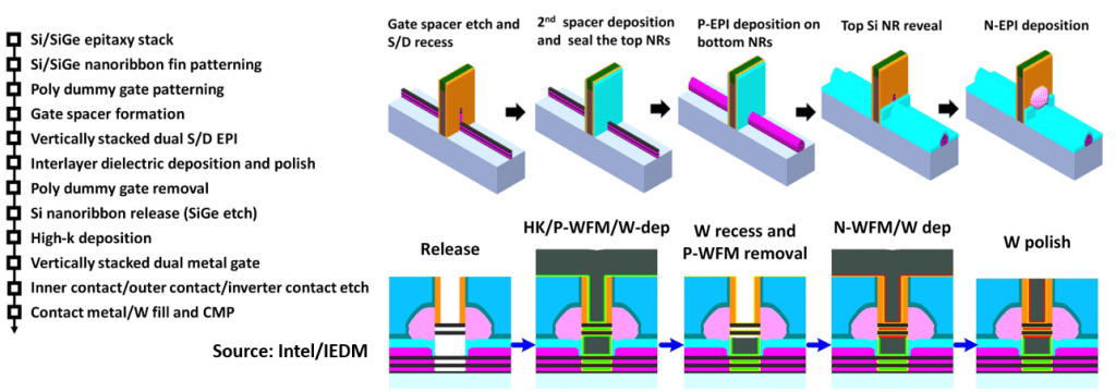
Note that the lower PMOS ribbons are left intact, but the top NMOS ribbons are removed except within the gate stack, then the N-epi is grown on the stubs of the channel ribbons. The dual work-function materials (WFMs) used requires the deposition of P-WFM and tungsten (W) first, then W back-etch to below the N-ribbons, leaving W covering the P-ribbons. Then the N-WFM layer is formed, followed by the final W deposition and CMP. With gate lengths of ≥30 nm, there should be no problems with W gate fill.
Ideally, we would expect the PMOS ribbons to be SiGe for better mobility, but that would complicate the initial epi stack and the subsequent ribbon release, so here we have the straightforward approach of Si PMOS devices. Intel has another paper on SiGe PMOS nanosheets (2.2 Gate-All-Around Strained Si0.4Ge0.6 Nanosheet PMOS on Strain Relaxed Buffer for High Performance Low Power Logic Application, Ashish Agrawal, et al.), as does IBM (2.3 Stacked Gate-All-Around Nanosheet pFET with Highly Compressive Strained Si1-xGex Channel, Shogo Mochizuki, et al.), but these will not be in complementary stacks.

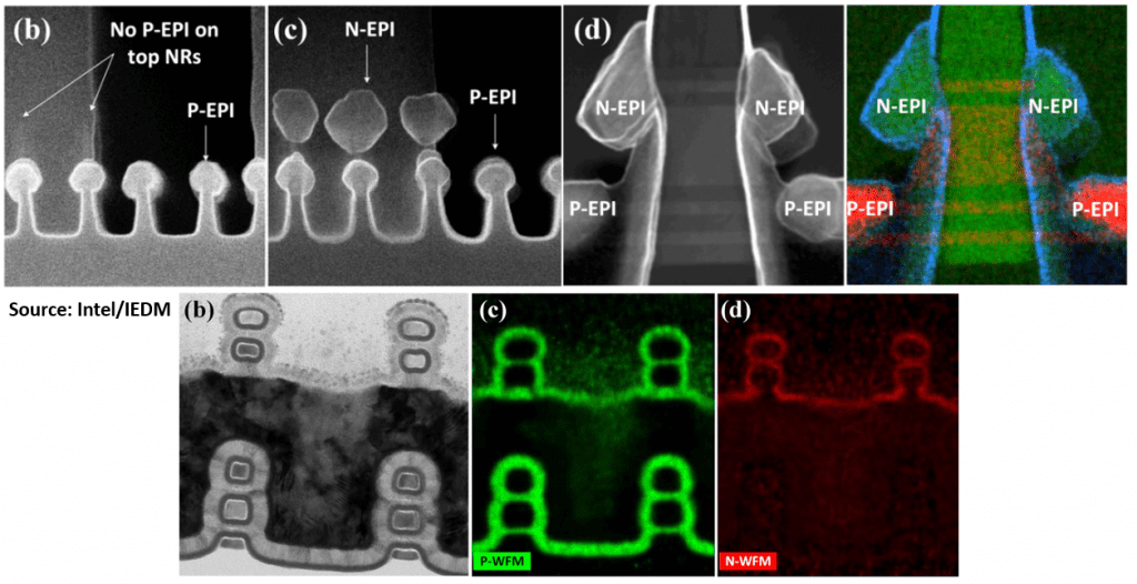
SEM image (b) in the top row above shows P-epi selectively grown on the bottom nanoribbons, then later in the sequence (c) shows N-epi selectively grown on the top two nanoribbons. The orthogonal views in (d) features SEM and SEM/EDS images showing selective N-epi and P-epi growth on the stacked nanoribbon transistors.
In the bottom row, (b) is a TEM cross-section image of the ribbons with WFM formed, likely before the second W deposition; (c) and (d) are TEM/EDS images of the dual metal gate, (c) showing P-WFM on the bottom nanoribbons, and residual P-WFM on the top two, and (d) showing N-WFM on the top two nanoribbons.
We will have to wait until the conference to see the performance characteristics, but this is an interesting proof-of-concept paper, and illustrates that there are still some stages to go before silicon technology runs out.
Now let’s look at the e-DRAM paper:
28.1 Anti-ferroelectric HfxZr1-xO2 Capacitors for High-density 3-D Embedded-DRAM, Sou-Chi Chang, et al., Intel Corporation
Again, quoting the abstract:
“3-D anti-ferroelectric HfxZr1-xO2 capacitors are demonstrated for eDRAM by showing (i) 10ns read/write operations, (ii) maximum operating voltage less than 1.8V, (iii) retention much longer 1ms, and (iv) endurance reaching 1012 cycles at 80C. Mechanisms behind endurance fatigue are discussed, and a novel architecture toward ultra-high density eDRAM is presented.”
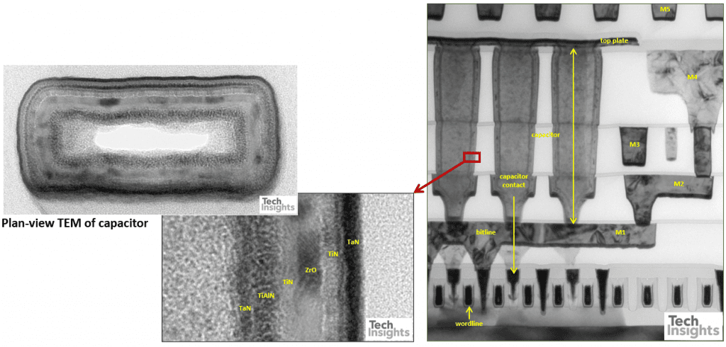
This is not the first time that Intel have developed e-DRAM [1, 2], though that was actually in a separate die introduced with the Haswell processor back in 2014. It was used as a 128 MB L4 cache, with a die size of ~79 sq. mm, co-packaged with the CPU. It featured a COB (cell over bitline) stack, with MIM capacitors in the metal-dielectric stack using cavities formed in the lower metal level dielectrics, and was (is?) fabbed in Intel’s 9-metal, 22-nm process.

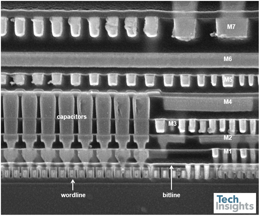
The MIMcap was formed from TaN/TiN/ZrO/TiN/TiAlN/TaN layers within the cavities etched as the metal stack is built up.

In the IEDM paper, Intel’s researchers used the antiferroelectric (AFE) material hafnium-zirconium-oxide (HfZrO2) to form a 3D deep-trench capacitor as a potential embedded DRAM memory cell. They also tried the HfZrO2 in a 3D stack with one wordline transistor accessing four AFE capacitors in parallel.

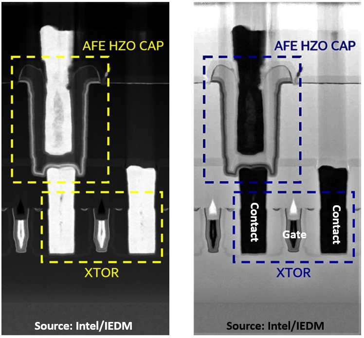
In the TEM images above, the left is the darkfield one from the IEDM tipsheet, and in the right I have reversed it to brightfield, marked the transistor elements, and optimized the contrast to try and clarify what we are looking at. The vertical streaks above the contacts are artefacts of the TEM sample prep technique. The capacitor itself is above the transistor, so while it might be trench-shaped it is not a conventional trench capacitor (in the substrate, as used by IBM down to the 14-nm node).
The tungsten plug in the center of the capacitor is likely connected to the common plate, though that is not shown here. The shape of the gate indicates it is a finFET transistor, but I cannot see any fin, so maybe this sample was taken in a field region; actually a useful way of looking at structures like gate and capacitor stacks.
In the 1T-4C stack shown below, it looks as though the common plate has been moved to the outside of the capacitor, and we have four horizontal levels (PL1 – PL4) surrounding the individual inner node plates. The schematic indicates that the capacitors are laid out like a DRAM, with two capacitors connected through a pair of wordlines to a shared bitline. The capacitors have been divided into rows by isolation trenches, and the common plates are contacted via a staircase structure much like a 3D NAND stack.

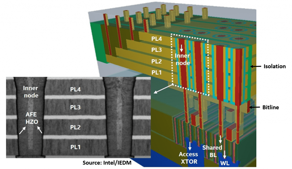
We don’t know any of the dimensions of the cells here, but the ability to stack common plates has to give a significant density advantage. If the memory characteristics are good, and the density can exceed the ~1.6 MB/mm2 of the existing eDRAM, then we could see this in the not-too-distant future.
As we said in the introduction, IEDM will be virtual this year, and the schedule is quite different. For the details, go to the program, tutorials, short courses, and plenaries pages on the website.
References
- R. Brain et al., A 22nm High Performance Embedded DRAM SoC Technology Featuring Tri-gate Transistors and MIMCAP COB, Proc VLSI Symp 2013, pp. 16-17
- Y. Wang et al., Retention Time Optimization for eDRAM in 22nm Tri-Gate CMOS Technology, Proc IEDM 2013, pp. 240-243.