By Dick James, Contributing Editor
Intel held their virtual 2020 Architecture Day on August 13th, hosted by Raja Koduri, and the first major topic was Process Innovations, with Ruth Brain as the presenter. Ruth started with a potted history of Intel processing, from the first strained channel at the 90-nm node to the string of 14-nm evolutions.

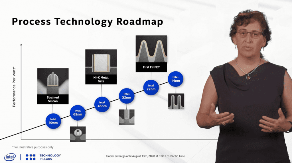
As we know, with the delay in yielding 10-nm, the 14-nm generation had four additional inconveniently named sub-nodes (14+ → 14++++), which actually boosted performance by more than 20%, equivalent to a full node progression.

Then a quick review of 10-nm so far, with its ambitious hyper-scaling factor of 2.7; as Ruth said, “it’s really no secret that we have had challenges bringing this process into production”. Comparing the Cannon Lake and Ice Lake 10-nm parts, TechInsights revealed at their IEDM reception last year that there were initial problems in the middle-of-line (MOL) and the contact-over-active-gate (COAG) parts of the 10-nm process.
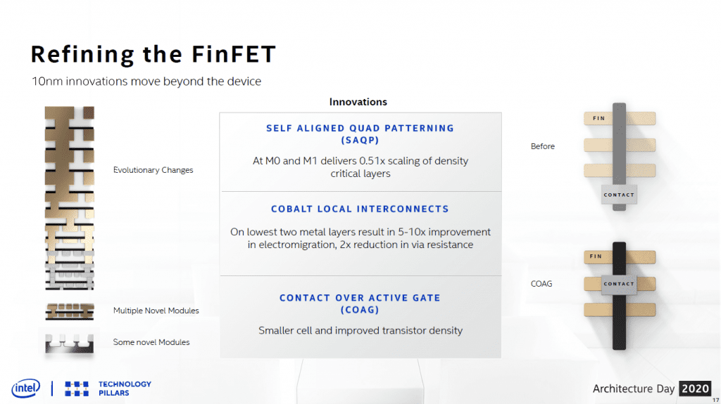
Ruth further stated that “ultimately we overcame these challenges and have introduced multiple products on this technology platform”, and indeed there are 18 versions of Ice Lake, Lakefield, and Snow Ridge listed on the Intel ark product listing website (at the time of writing). So presumably the SAQP, COAG, and cobalt will stay as part of the what is now the base 10-nm process.
SuperFin Transistor
Now we get to the meat of her talk – the updated “SuperFin” technology. I took the trouble to transcribe what she said:
“Within the transistor, we improved epitaxial growth of crystal structures on the source and drain, increasing the strain and reducing resistance. It allowed more current to flow through the channel. We had an enhanced source/drain architecture driving additional higher channel mobility, enabling charge carriers to move more quickly. Additionally, we had a gate pitch that we have included, to provide higher drive current for certain chip functions that require the utmost performance.”

In a later session discussing Tiger Lake, Boyd Phelps gave us his spin on SuperFin:
“We added a new high-performance transistor that increases drive current with an improved gate process enabling higher mobility while also lowering the source/drain resistance, and we did this all with lower capacitance.”
Parsing these two statements, it seems we have some process tweaks in the front end:
- Modified epitaxial growth of the source and drain, increasing strain and reducing resistance;
- Enhanced source/drain architecture to give higher mobility;
- An updated gate process also increasing mobility;
- Lower capacitance in the transistor structure
All of which gives me the irresistible urge to speculate what those changes might be!
Let’s take them in the above sequence, starting with the modified epi. For PMOS, the Ge content in the SiGe source/drains is already 50% or greater, and it seems unlikely that you could cram much more in without increasing the risk of creating lattice defects at the Si/SiGe interface.
However, the Ge content that I’ve seen is usually graded, with the maximum at the contact, and noticeably less at the interface. Changing the epi growth to put more Ge closer to the interface should increase the channel strain. It’s lost in the mists of time now, but one of the original reasons for going to e-SiGe was that it allows higher boron doping, so in addition to increased strain, increased Ge could also enable an incremental boost to the S/D doping level.
When it comes to NMOS it has never been established that Intel has used carbon doping in the source/drains to induce tensile stress, but if they have now managed that, it will enhance NMOS mobility. The original technique of silicon nitride sidewall-induced tensile stress has been virtually eliminated since there is so little of it there, now we are down to ~50 nm CPP.
Epitaxial architecture is specifically mentioned, which makes me wonder if the S/D cavity etch has been altered to give a more ∑-etched cavity, putting the SiGe/Si:C closer to the channel, again upping the strain and thus mobility. Not easy to do in a fin ~6-7 nm thick, but it should work.
Boyd Phelps mentioned “an improved gate process enabling higher mobility”; I can’t think of how the gate stack itself can increase mobility, unless somehow the gate fill could build z-stress into the gate, but in a 16-18 nm gate length there’s not much room for stressor materials.
Thinking back to planar days, strain was “memorized” in the channel by using a sacrificial layer of stressed nitride before the source/drain engineering; maybe in the polysilicon dummy gate process, before S/D formation, Intel have found a way to memorize stress in the channel, to add to the S/D generated stress.
Capacitance has also been lowered – that could be a result of the larger gate pitch mentioned, but we could also have sidewall spacers with a lower dielectric constant, or even air gaps – IBM had a paper at this year’s VLSI describing a 15% reduction in Ceff [1], and Samsung used them in their 20-nm DRAM technology [2].

There are other changes that could have been introduced that are not mentioned, such as taller fins (perhaps unlikely since we are already over 50 nm), and/or SiGe fins for PMOS, though I would think that’s more likely at 7-nm.
The 10-nm base process was announced [3] with six Vt options, and Boyd Phelps also claimed that the introduction of the new high-performance transistor allowed some of the existing high-Vt devices to be tweaked to run at higher frequency with lower leakage, so their operating voltage could be reduced, making more power available for high-performance sectors.
SuperFin MIM-Cap
Going back to Ruth brain’s talk, she also said:
“Moving up to the metal stack, a new thin barrier reduces via resistance by up to 30%, enhancing interconnect performance. The final innovation is new super-MIM (metal-insulator-metal) capacitor. When compared to the industry standard, it delivers a 5x increase in capacitance in the same footprint, driving a voltage reduction that translates to dramatically improved product performance. … This innovation is enabled by a new class of high-k dielectric materials stacked in ultra-thin layers, just several Ångstroms thick, to form a repeating super-lattice structure.”
And Boyd added:
“We invested significant engineering focus and resources to redesign the metal stack as well. We greatly improved the resistance, the availability, and yield-ability of the mid-layers. We also added two additional high-performance layers at the top, and dramatically enhanced the MiM-cap capabilities to ensure a rapid and solid power delivery response for high-CPU intensity workloads.”
So, in the back end we have:
- Thin barriers in the vias, reducing resistance by up to 30%;
- Super MIM-cap with dielectric formed of multiple sub-nanometer layers;
- Two extra high-performance metal layers at the top of the stack

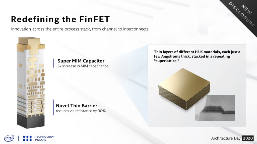
Squinting at the metal stack in the above, I think I can see 18 metal layers, including M0, five more than the initial 10-nm offering in [3], and four more than the first 10-nm slide above, assuming the schematics are accurate. It also appears that the MIM-cap is between M16/M17, and the thin-barrier vias seem to be at M5 and below.
No details were given of course; but I did find a reference for improved via resistance from IITC 2016 – the via dielectric is plasma nitrided before deposition of pure tantalum, giving a thin TaN barrier, and reducing via resistance by 30% [4]. I’m tempted to wonder if the new selective tungsten gap-fill technology from the Applied Materials Endura Volta system may be being introduced, but that would be zero barrier, and it’s likely a bit early for volume introduction.
The Ångstroms-thick layers of the Super MIM-cap reminded me of another Applied materials launch, at last year’s Semicon West. This was the Endura Clover MRAM PVD platform, specifically designed for the “precise deposition of at least 30 different layers of material, some of which are 500,000 times thinner than a human hair”. If you take a human hair thickness as ~100 µm, that means layers ~2Å thick.
Given that MRAM materials can also have healthy dielectric constants, it seems likely that such a system could be used for the Super MIM-cap. Or there’s regular ALD, as used in DRAM dielectrics, which have ZAZ (Zirconia/Alumina/Zirconia) layers in the capacitors. The figure below shows a comparison of the schematics:

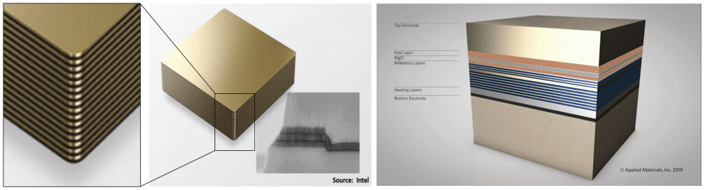
By my count there are 32 layers in the Intel schematic, so with 2Å layers ~6.4 nm total thickness if the schematic is accurate. The inset TEM shows a three-layer capacitor, with what looks like TiN electrodes; the dark lines are the dielectric layers, presumably with the multi-layer structure. On the right the Applied Materials schematic illustrates the multi-layer MRAM stack formed by the Clover system.
The last change mentioned was the extra two high-performance metal layers at the top of the stack; given that they should be the largest, they should be relatively high performance, though there could be tweaks like tuning the grain structure, or adding cap/liner layers to improve electromigration properties.
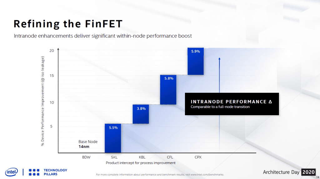
Taken together, Intel claims that the transistor, capacitor, and metal stack changes make the largest single intra-node improvement in the company history, ~18% according to the plot below.

Also coming up, there is already an “Enhanced SuperFin” variant being developed with yet more optimized transistors and changes to the metal stack, aimed at data centre products.
Nomenclature
As we noted above, at the 14-nm generation the ‘+’ notation became definitely clunky, and at 10-nm we got even more confused with the brief introduction of the Cannon Lake product. It now appears that Intel is regarding the Ice Lake process as the baseline, so the SuperFin version is the equivalent of 10+ (Cannon Lake was 10- ?).
Quoting Raja Koduri:
“In fact, during 14-nm generation, there were so many pluses, that we often internally mixed up the actual plus count. Left unchecked, we were going down the same path with our intranode improvements in 10-nanometer. … So we decided, internally, to stop using the plus-plus nomenclature, and get to a descriptive and memorable name to denote and celebrate significant internal enhancements. Taking advantage of the SuperMIM capacitor and the enhanced finFET, we decided to call the generation of transistors SuperFin.”

To me, SuperFin as a name implies only changes to the transistor, even just the fin of the transistor, and gives no clue to the other innovations in the back end, so it’s almost as confusing as the plus terminology. It is a convenient abbreviation, though – 10SF is like the foundries’ 7FF or 7LPP, and could morph to 10ESF or 10SFE for the enhanced version. We’ll see if it survives…
The debut of 10SF will be in the Tiger Lake SoC, due to be launched on 2nd September, and I guess they’d like to have the laptops in stores for the holiday period. We look forward to it!
Addendum – Agilex FPGA
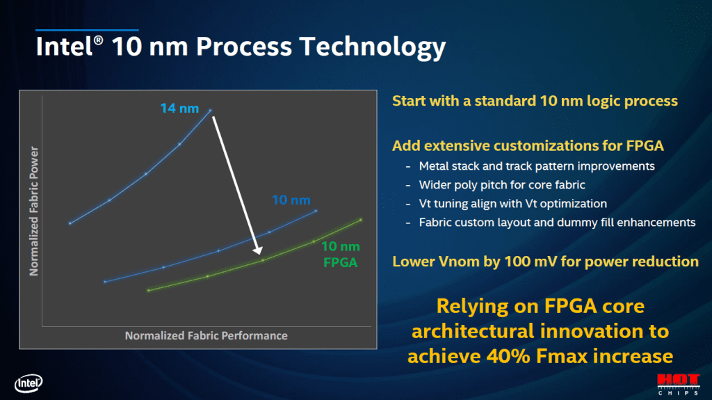
The week after the Architecture Day, the Hot Chips 32 virtual conference took place, and Intel presented on their Agilex FPGA family, and noted that they use a customized 10-nm process.
It doesn’t appear that this pushes into the 10SF upgrade, but will be yet another variant to watch for, now they have started shipping.
References
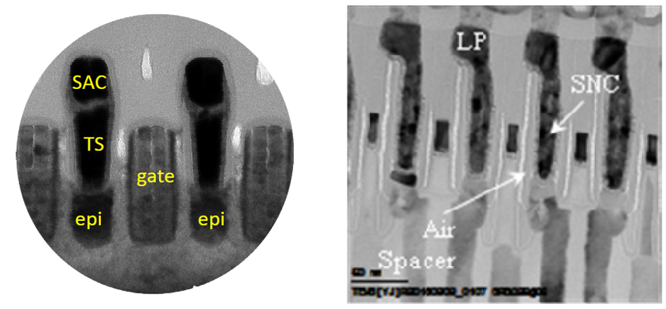
- K. Cheng et al., “Improved Air Spacer Co-Integrated with Self-Aligned Contact (SAC) and Contact Over Active Gate (COAG) for Highly Scaled CMOS Technology”, VLSI 2020
- J.M. Park et al., “20nm DRAM: A new beginning of another revolution”, IEDM 2015, pp. 676 – 679
- C. Auth et al., “A 10nm High Performance and Low-Power CMOS Technology Featuring 3rd Generation FinFET Transistors, Self-Aligned Quad Patterning, Contact over Active Gate and Cobalt Local Interconnects” IEDM 2017, pp. 673 – 676
- C.-C. Yang et al., “Pre-liner dielectric nitridation for resistance reduction in copper interconnects”, IITC 2016, pp. 89 – 91