By Dick James, Contributing Editor
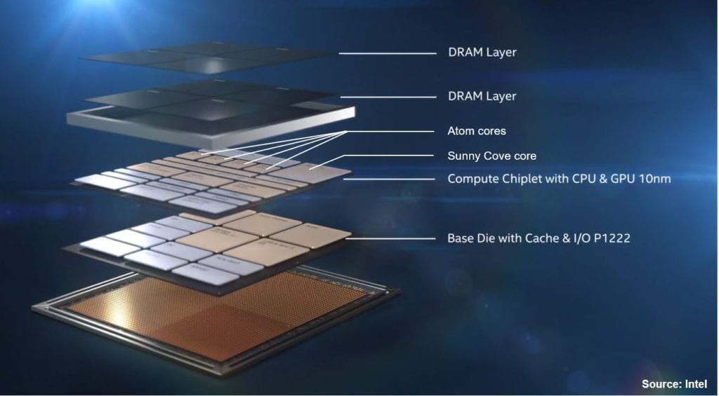
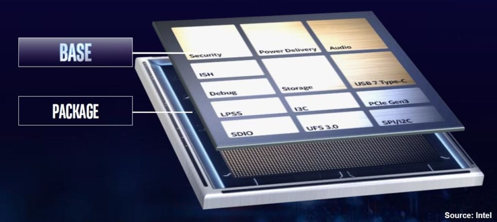
At the Architecture Day Intel demoed a Foveros-based part, comprising a high-performance 10-nm chiplet on a low-power 22nm base die. The upper die contained five cores, four Atom low-power cores and a high-performance core, and as shown in the Intel image above, the two lower dies were stacked with PoP memory, all in a 12 x 12 mm package with 2mW standby power.

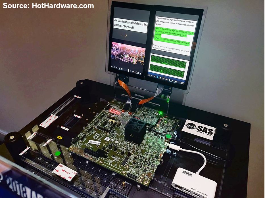

Products using the Foveros technology were expected to be shipped in 2H19. More information was given at CES, when the hybrid Lakefield CPU(four Atom cores and a Sunny Cove core in a 12 x 12 mm package) using Foveros packaging was announced. It looked remarkably similar to the package:

No mention was made of the amount of memory on board, but the following still from the CES video indicates eight dies – these days, that could be 8 x 8 Gb, so 8GB. Again a 2H19 ship date was predicted.

Murthy Renduchintala discussed Lakefield again at the Intel investor meeting in May, showing a bit more detail of the base die:

Which gives an indication of the design and test complexities – sub-dividing the IP blocks between the chiplets, as well as the P1274 and P1222 processes, ensuring the clocks and interconnect all work, and re-jigging the testing so that the chiplets are known good dies; and then of course testing the whole assembly for functionality, with and without the DRAM.
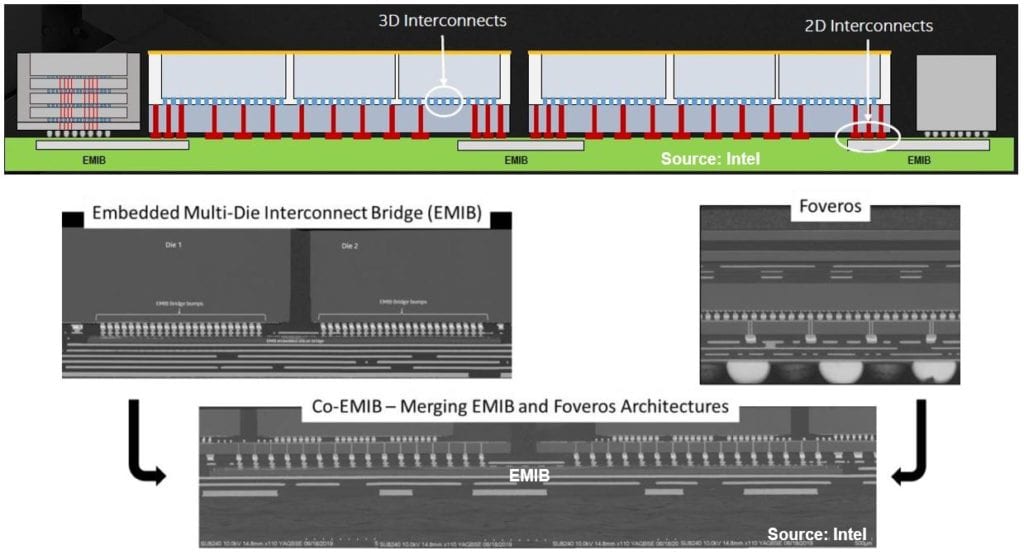
That takes us to the Advanced Packaging Workshop held by Intel on the Monday before the Semicon West show (July 8). Intel announced three new developments – Co-EMIB, Omni-Directional Interconnect (ODI), and MDIO.
Co-EMIB essentially combines the Foveros die stacking and active interposer with the EMIB bridge dies; below is a schematic cross-section and some Intel cross-sectional images of EMIB, Foveros and Co-EMIB:

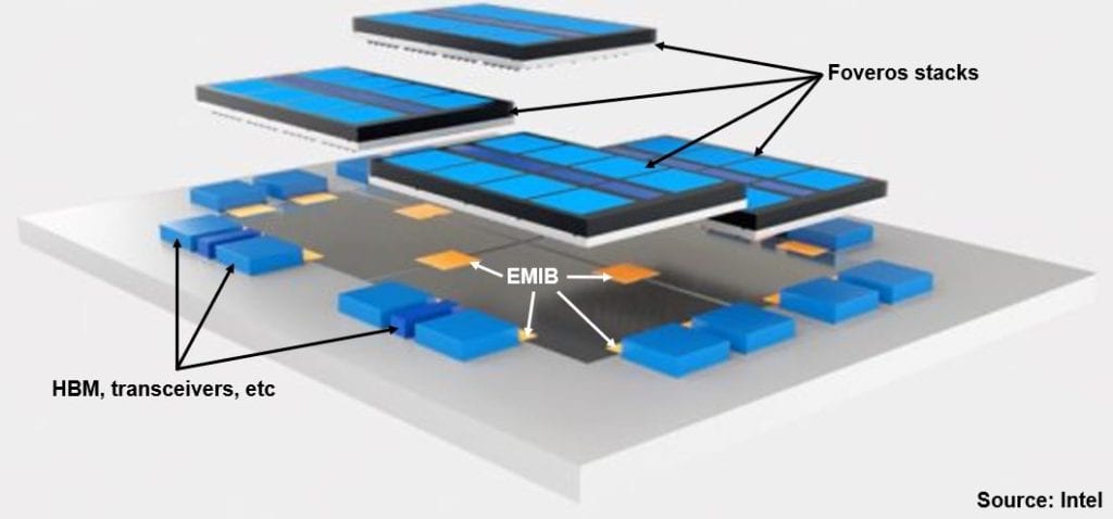
The above cross-sections only show a few dies, but Intel posted a short videowhich shows conceptually what could be done, and I have annotated a still shot from it below.

Co-EMIB features high-density interconnect, with the EMIB die having a bump pitch of 55 µm, and the Foveros stack 50 µm, projected to go to 30-45 µm and 20-35 um respectively. EMIB has 256 I/Os/mm/layer, which works out at a line/space of 2/2 µm; a bump pitch of 50 µm gives us 400 I/Os/mm2.
The second announcement, Omni-Directional Interconnect, seems to be a combination of EMIB-style interconnect using part of the active interposer, and through-mold vias (TMVs) to deliver power directly to the chiplets on top of the interposer. Intel again posted a video, and again here is a marked-up screen shot:

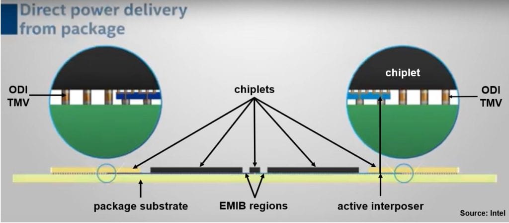
It is worth noting that in this illustration the outer chiplets overhang the edge of the interposer and the TMVs connect to them in the outer part of the package. The interposer could also be so small that it only functions as an EMIB (but not embedded in the substrate), or for direct ODI connection to every chiplet there could be multiple interposers containing the base logic that are smaller than their respective chiplets. In all these variants the large TMVs have lower resistance than TSVs through the interposer, giving better power delivery and still having the higher bandwidth and lower latency from the Foveros stacking. It also reduces the number of TSVs in the interposer die, allowing smaller die size or more active transistors.
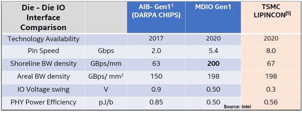
Lastly, Intel revealed a new chiplet/chiplet interface, MDIO, developed from their Advanced Interface Bus (AIB) PHY-level interconnect. MDIO (variously translated in the media as Multi-Die I/O or Management Data I/O) increases the pin speed from 2 to 5.4 Gbps, and reduces the I/O voltage swing from 0.9V to 0.5V, and the picojoule/bit from 0.85 to 0.50. This was claimed to be comparable to the TSMC LIPINCON interface detailed at this year’s VLSI Circuits Symposium [5].

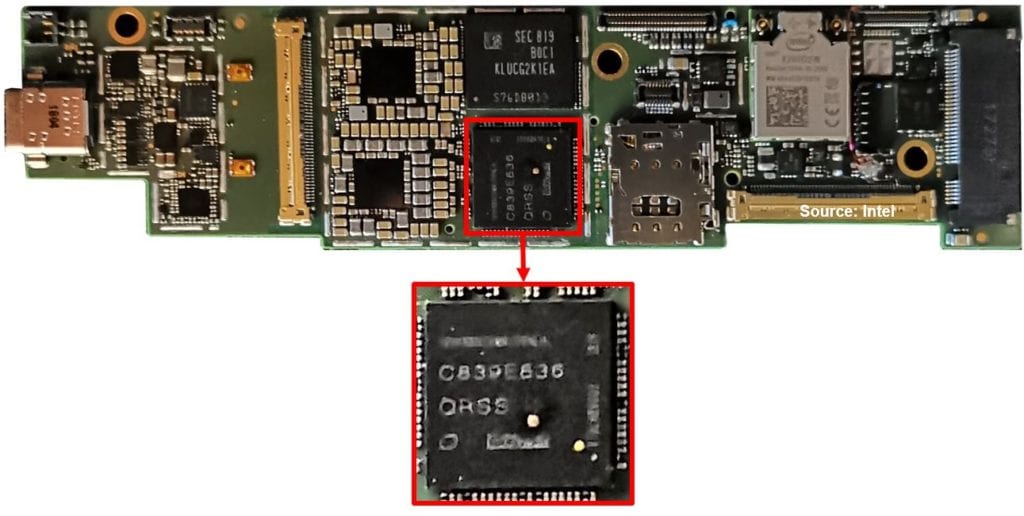
One of the luxuries of reviewing announcements after the event is that we can sometimes see what may not have been detailed in the rush of the presentation; in this case, what looks like a cross-section of a Lakefield part.

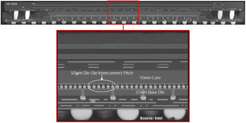
The LKF-2018 marking at the top left of the upper image seems to confirm that speculation.
While all the above is remarkable, if not amazing, Intel seems to have “kept their light under a bushel” in terms of their packaging development; most, if not all, of the commentary about the company focuses on the chip architecture or process. Meanwhile, a bunch of folks in Chandler, Oregon, and Malaysia have been plugging away for a good long while at developing assembly and test technologies, and only occasionally attract attention. For me, a good part of the story is this culmination of the work that they have been doing for the past couple of decades at least.
Part 3 Coming Soon