By Dick James, Contributing Editor
The SEMICON West workshop was unusual in that all the presenters were from Intel’s Assembly Test Technology Development (ATTD) group, and the session kicked off with a review of ATTD by Corporate VP Babak Sabi.
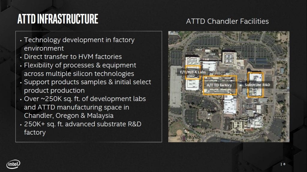
The scope of their activities ranges from wafer sort, die preparation, and identifying known good die, through assembly, test, die finish, and board development, and also substrates, tooling, and other assembly materials; so pretty well the whole spectrum. They have quite the complex in Chandler (Arizona), as well as other facilities in Oregon and Malaysia.

Current focus, which isn’t much narrower than the above scope, is on:
- Thin/small footprint client packages
- Power delivery architectures
- Thermals
- High speed signaling
- Interconnect scaling density and pitch
- Tech portfolio
- IDM and co-design
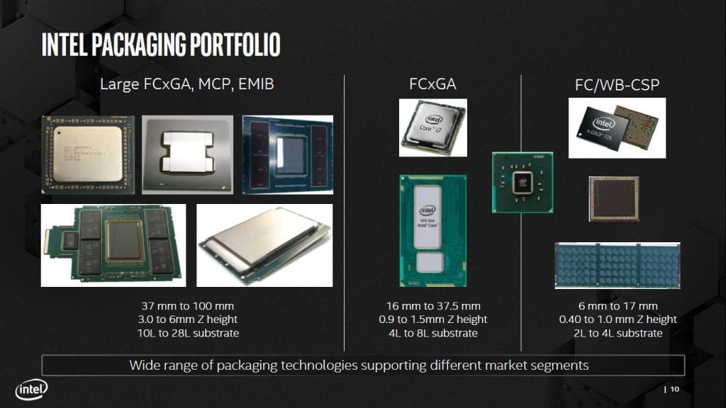
And some of the packages that we have seen in recent years were detailed:
But as I said earlier, for me Intel’s package developments are a long-running story, if low-key. In 2001, Anandtech reported on their “Bumpless Build-Up Layer” (BBUL) technology, and commented that the Assembly Technology Development group was 900 people back then. (BBUL was reported on in the previous year [6], and in retrospect almost looks like the current fan-out wafer-level package.)

If we just look at the precursors for the latest announcements, Intel was working on wafer stacking as far back as 2004 [7], and Bill Holt showed off F2F Cu/Cu wafer stacking with TSVs at the Hot Chips conference the following year [8].

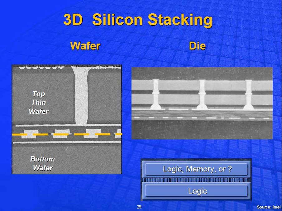
The above is clearly a test structure, but it didn’t take long to get some SRAM bonded and tested [9]. 300-mm, 65-nm technology wafers with test transistors and 4-MB SRAMs were bonded face-to-face using copper pads of sizes 5×5 μm to 6×40 μm, and the upper wafers were thinned to 5 to 28 μm thick.

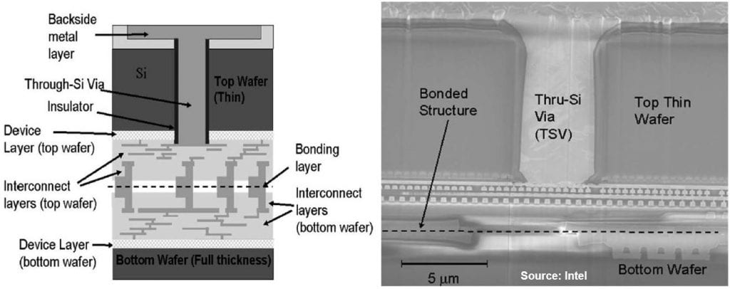
The circuits on the upper part were tested through the TSV and backside metal layer, and those on the lower part were tested through the TSVs and the Cu/Cu bonds, with no degradation in performance compared with un-bonded control devices.
This 3D-stacking activity was included in the Tera-scale computing project run by Intel in the mid-late 2000s, which had an 80-core processor designed to give a teraflop at the power level used by a desktop, and to utilise stacked memory.

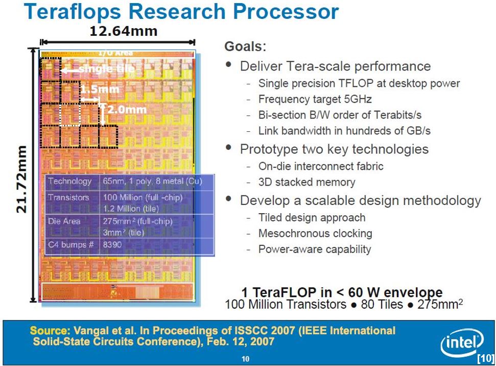
In 2007, I attended the Intel Developer Forum, and one of the displays that caught my eye then was a wafer of alternating (65-nm) SRAM and the 80-core processor dies, with a working demo of the Terascale processor running at >1 – 2 teraflops, using 100-200W.
The SRAM parts on the demo wafer were laid out to allow for through-silicon vias or face-to-face stacking with the processor die. As of then, I had not realized that Intel had been doing so much package development, but talking to them, their guys in Arizona had all the infrastructure to handle 70-micron-thick dice and stacked packaging – for them, it was not how to do it, it was when.
Phil Garrou of the IFTLE blog noted that during the 4th 3D-ASIP conference in December 2007, Intel’s Jerry Bautista commented that there were no remaining technical issues and that Intel was ready to commercialize their 3D integration technology “…as soon as the product groups decided which product to insert the technology into.”
Given that we are now twelve years further on, presumably Lakefield is the first product that has crossed the cost/performance threshold to justify using 3D stacking, such are the gains from 2D scaling and the architectural evolution that we have seen in the last decade or two.
Although EMIB was first announced in 2014, it was also the result of several years development. Simulations and a test vehicle were reported in 2011 [11], although it was known then just as a “silicon bridge”. 2/2 µm lines/spaces and bump pitches of 30 – 50 µm were evaluated, and the active dies had both regular-pitch and fine-pitch bump fields.

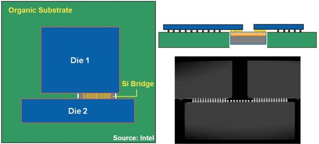
The conclusion was that it was a concept that looked promising, though with the caveat that “Major challenges and unknowns to be investigated further include package reliability, assembly through-put achievable in high-volume manufacturing, precision substrate through-hole formation, and die/package co-design implications.” Clearly those problems were solved.
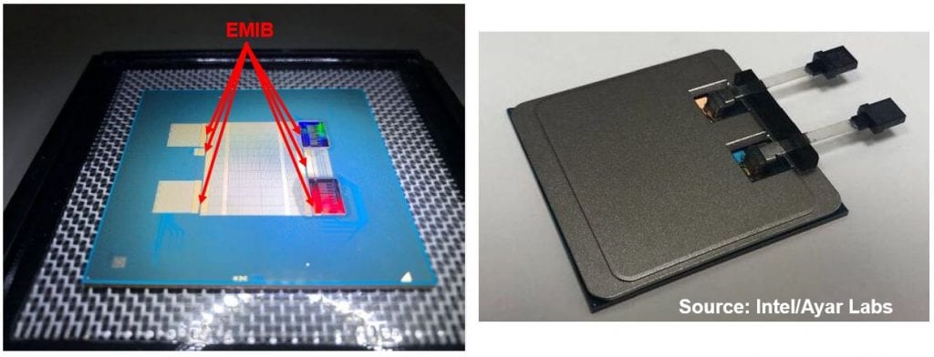
EMIB is expanding its usage to the photonics field now; in another talk at Hot Chips 2019, Ayar Labs is working with Intel to use it to connect their TeraPHY optical interface chips to an FPGA, as part of a DARPA project [12].
Which just about brings us up to date; the ATTD group at Intel has been doing solid work for decades, and while we have seen a flurry of Intel announcements on heterogeneous integration in the last year or so, clearly they are the culmination of more than ten years concentrated effort.
To conclude, since I didn’t make it to any of the briefings described above, I have to thank my colleagues in the semiconductor press, and Intel for making the slide decks available, and also TechInsights for the chip analyses included.
References
- “Intel Announces New Packaging and Test Technologies for Foundry Customers”, Intel press release, Aug. 27, 2014
- R. Mahajan, “Localized High Density Interconnects with Intel’s EMIB”, IMAPS 12th International Conference and Exhibition on Device Packaging, March 14 – 17, 2016
- https://www.intel.ai/nervana-engine-delivers-deep-learning-at-ludicrous-speed/#gs.tyi1jq
- A. Yang et al., “Deep Learning Training At Scale – Spring Crest Deep Learning Accelerator”, Hot Chips 31, 2019
- B. Sell, et al., “22FFL: A High Performance and Ultra Low Power FinFET Technology for Mobile and RF Applications”, IEDM Tech. Dig. 2017, pp. 685 – 688.
- M. Lin, et al., “A 7nm 4GHz Arm core based CoWoS chiplet design for high performance computing”, VLSI Symp. 2019, pp. C28 – C29
- S. Towle et al., “Bumpless Build-Up Layer Packaging”, Proc. ASME Int. Mech. Eng. Congress and Exposition (IMECE), 2001
- P. Morrow et al., “Wafer-level 3D interconnects via Cu bonding”, Proc. AMC, 125-130 (2004)
- https://www.hotchips.org/wp-content/uploads/hc_archives/hc17/2_Mon/HC17.Keynote/HC17.Keynote1.pdf
- P. Morrow et al., “Three-Dimensional Wafer Stacking Via Cu–Cu Bonding Integrated With 65-nm Strained-Si/Low-k CMOS Technology”, IEEE Electron Device Letters, Vol. 27, no. 5, May 2006, pp. 335 – 337
- H. Braunisch et al., “High-Speed Performance of Silicon Bridge Die-to-Die Interconnects”, EPEPS 2011, pp. 95 – 98
- M. Wade et al., “TeraPHY: A Chiplet Technology for Low-Power, High-Bandwidth Optical I/O”, Hot Chips 31, 2019