BY DICK JAMES, Contributing Editor
In the last several years, Intel has had a series of announcements in the packaging arena, focused on the integration of multiple styles of chips in the same package to improve performance and broaden system capabilities.
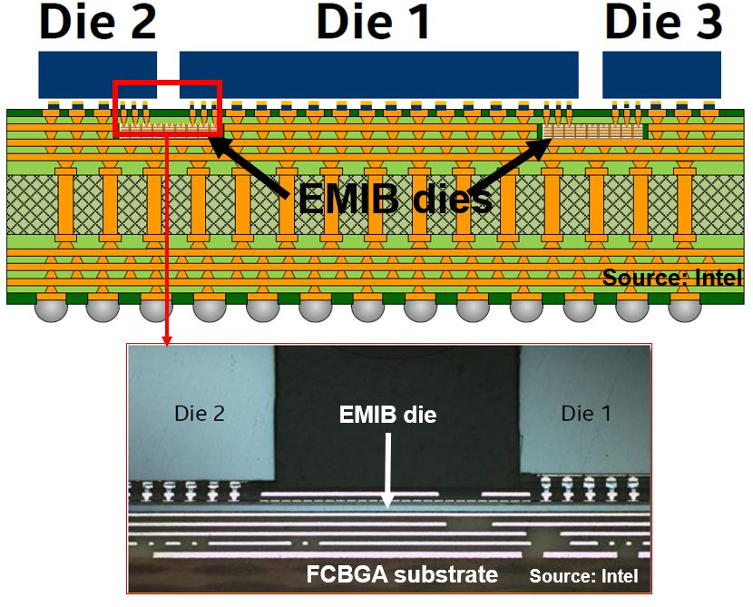
The first of these was EMIB (Embedded Multi-die Interconnect Bridge), launched in August 2014 [1] and detailed at that year’s IDF. The EMIB is a small silicon chip embedded in the underlying package substrate, incorporating ultra-high-density interconnect between the dies attached to it.

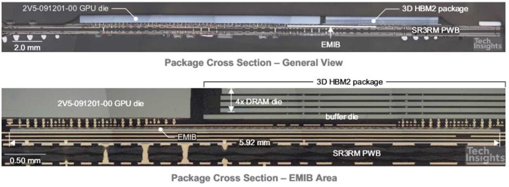
The initial announcement was as part of Intel’s foundry platform, which at the time included Altera as a customer, before they were absorbed by Intel. It took a while to bring it to a product, and the first consumer use of EMIB that I know of was last year, in an 8th Generation Intel® Quad Core™ processor with a Radeon™ RX Vega M GL GPU, linked by EMIB to 4 GB of HBM2 memory.

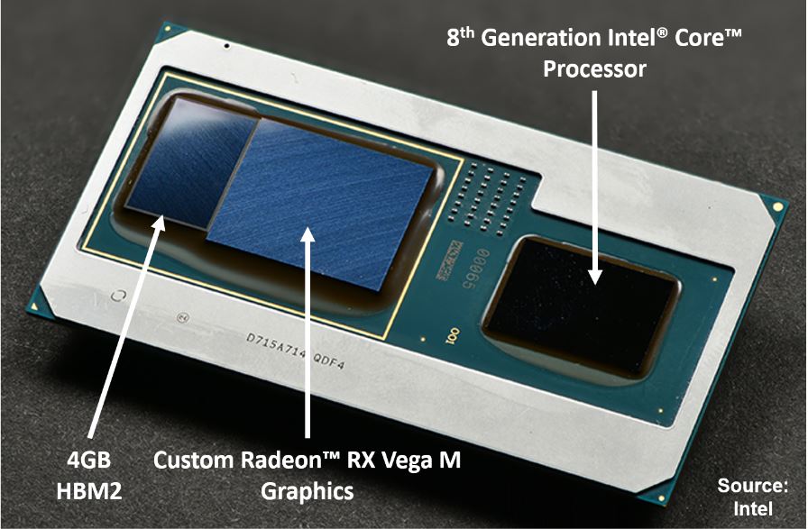
Intel claimed that this integration saved 1900 mm2(3 in2) of board area and reduced the package height to 1.7 mm, while taking up 80% less power than the GDDR5 equivalent.
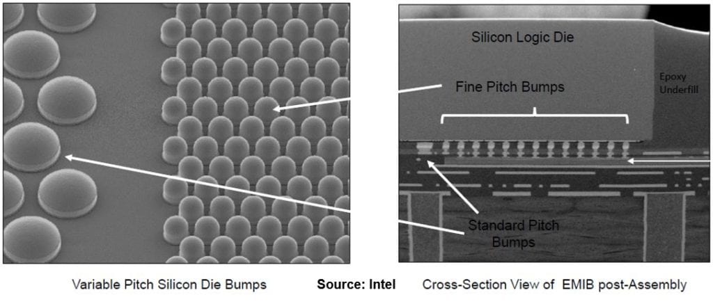
TechInsights looked at the i5-8305G (SR3RM) version, and in the following cross-section we can see (if we squint hard) that the EMIB die has five copper layers, including the bond pads, and the substrate is a 4+4 PWB. If we use the scale bar as a rough calibration, the die thickness comes out at ~32 µm, and the microbump pitch at 50 – 55 µm.

Almost simultaneously the Stratix 10 FPGA (launched as Altera, now Intel) came on to the market using EMIB as an interface between the FPGA die and the transceiver die:

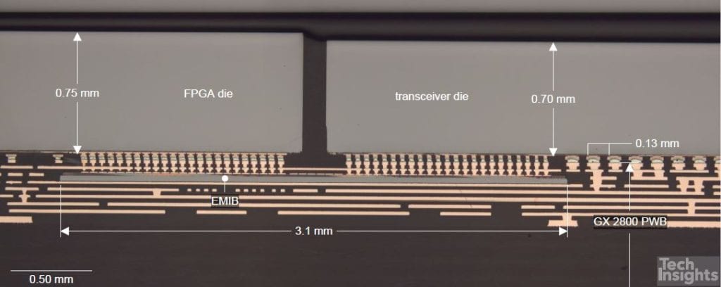
To optimize the number of I/O’s to the adjacent die, and therefore the bridge die, two bump sizes and pitches are used [2]:

After the EMIB announcements things went quiet for a few years, although it appears that following the acquisition of Nervana in 2016, Intel is using 2.5D silicon interposers for their Nervana neural network processor, with 32 GB of HBM2 memory [3].

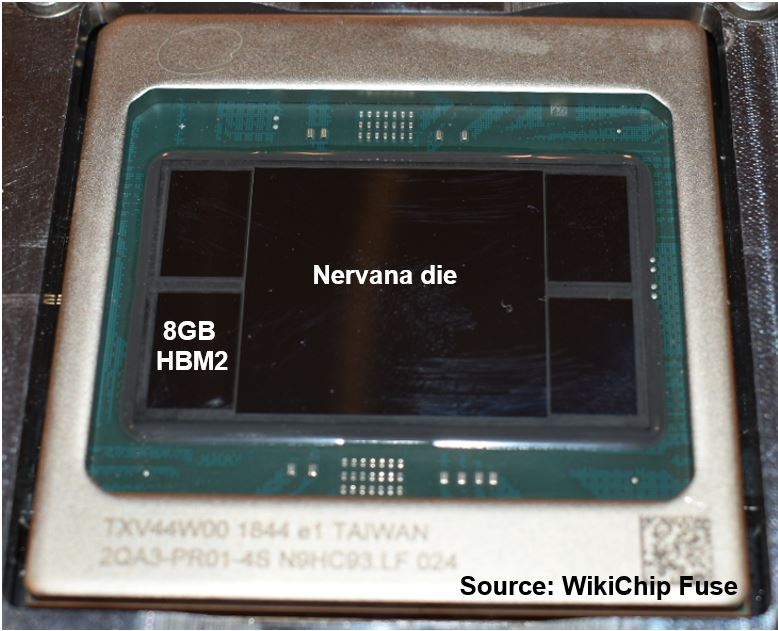
This appears to be an experimental product at the moment, since I can find no reference to commercial product being shipped, but samples have been sent out to potential AI customers such as Facebook. At the recent Hot Chips 2019 conference, Intel revealed [4] that the latest iteration is fabbed in the TSMC CLN 16FF+ process, so it seems likely that the packaging uses TSMC’s CoWoS technology. Die size is 680 mm², with a 1200 mm² interposer. This now seems to have been re-branded NNP-T (training) from NNP-L (learning), and the latest comment is that Baidu is collaborating with Intel on its development. There is another version, dubbed NNP-I (inference), that is a modified 10-nm Ice Lake chip, but that is a single die without any HBM. Be that as it may, Intel are at least dabbling with interposers, even though the sales pitch for EMIB is that it is cheaper and easier than huge slabs of silicon.
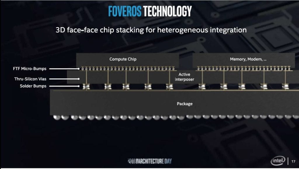
Last December Intel held their Architecture Day, and Raja Koduri disclosed the Foveros™ technology, which combines face-to-face (F2F) micro-bumping of multiple dies on an active interposer, with TSVs connecting them to the package substrate.


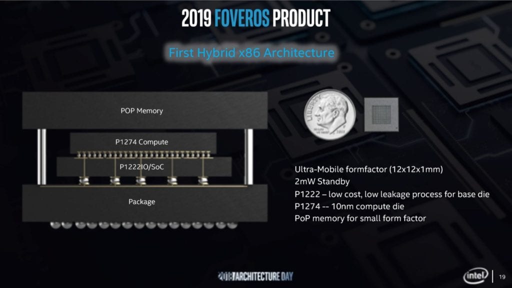
This can be used in a Package-on-Package (PoP) stack to give a hybrid structure:
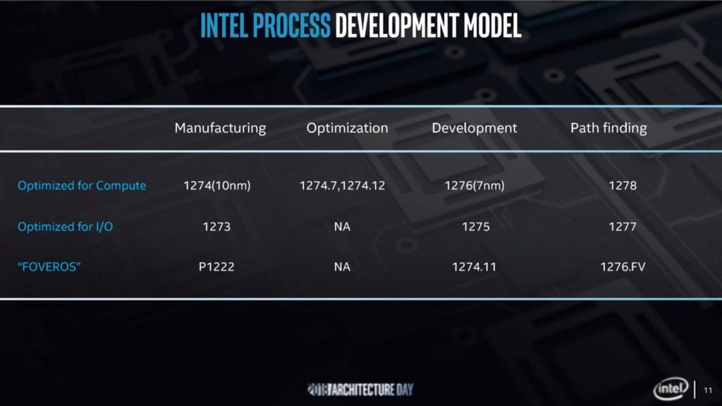
P1274 is Intel’s 10-nm process, P1222 is the 22FFL low-power process outlined at IEDM17 [4]. Judging by the following slide, the intent is to move the interposer die to a version of the 10-nm process, and then the 7-nm:
Of course, neither TSVs or F2F bumping are new, but the use of an active interposer is – to my knowledge, the CoWoS interposer and its equivalents are all passive interconnect die. F2F goes back commercially to 2006, when Sony used it in their PlayStation Portable; I have no images of that, but TechInsights (then Chipworks) looked at the PlayStation Vita back in 2012.
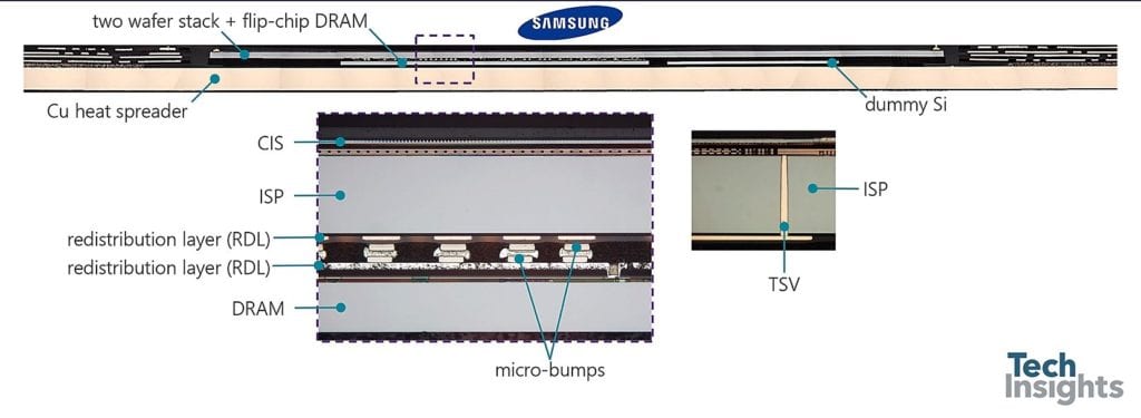
At the base of the stack we have the processor chip, with face to face to it a Samsung 1-Gb wide I/O SDRAM; and the top three dies comprise two Samsung 2-Gb mobile DDR2 SDRAMs, separated by a spacer die, and conventionally wire-bonded. The base die is ~250 µm thick, and the others ~100 – 120 µm.
More recently Samsung have used both F2F bumping and TSVs in their camera chip in the Galaxy S9, including a DRAM in a three-layer stack, to allow super-slow-motion imaging (~960 fps!).

Part 2 Coming Soon…