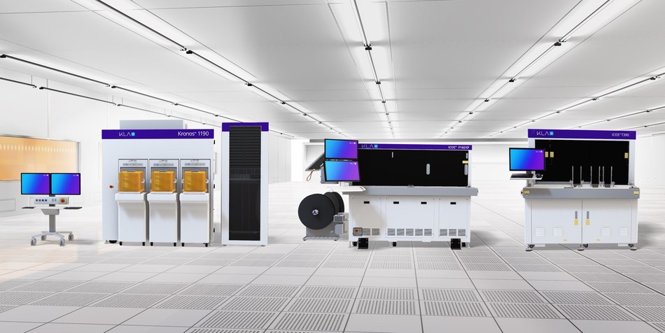
Today, KLA Corporation (NASDAQ: KLAC) announced the launch of the Kronos™ 1190 wafer-level packaging inspection system, the ICOS™ F160XP die sorting and inspection system and the next generation of the ICOS™ T3/T7 Series of packaged integrated circuit (IC) component inspection and metrology systems. The new tools’ increased sensitivity, improved throughput and enhanced, next-generation algorithms are designed to advance semiconductor device fabrication at the packaging stage by addressing the complexities of shrinking features sizes, 3D structures and heterogeneous integration. With the ability to implement these advanced packaging techniques more reliably, KLA customers will be able to improve device performance without relying on scaling silicon design nodes. The enhanced portfolio’s performance improves both yield and quality assurance, further enabling customers to advance their technology and cost roadmaps.

“Process control across all stages of packaging manufacturing, from wafer- to component-level process steps, becomes more critical as innovations continue to advance packaging technology. Our newly launched products help device manufacturers, foundries and outsourced semiconductor and test (OSAT) providers meet expectations for quality and reliability in an increasingly diverse and complex packaging segment,” said Oreste Donzella, executive vice president of the Electronics, Packaging and Components (EPC) group at KLA. “At KLA, we see a unique opportunity to leverage our 40+ year history of innovating semiconductor front-end fabrication technologies to further accelerate packaging yield through advanced process control solutions.”
The Kronos 1190 wafer inspection system utilizes high-resolution optics to provide inline process control for advanced wafer-level packaging process steps as features shrink and patterns become denser. Its DefectWise™ system integrates Artificial Intelligence (AI) as a system level solution, delivering a boost in sensitivity, productivity and classification accuracy. These improvements ensure that defects are correctly identified and sorted for superior quality control and yield learning. The new Kronos system also introduces DesignWise™, which adds design input to the FlexPoint™ precisely targeted inspection areas, improving precision over the inspection area and providing more relevant inspection results.
The ICOS F160XP system performs inspection and die sorting after wafer-level packages are tested and diced. High-end packages, such as those used for mobile applications, can suffer from dicing induced laser-groove, hairline and sidewall cracks due to their brittle materials. These cracks are not detectable with traditional visual inspection. The ICOS F160XP system includes the new IR2.0 inspection module, which combines optical and true IR side inspection, doubling the throughput for 100% IR inspection compared to the previous generation. This module provides an efficient inspection flow with high sensitivity to yield limiting cracks and other defect types, and accurately identifies bad parts for maximum die sorting accuracy.
The next generation of the ICOS T3/T7 Series features several new configurations of fully automated optical IC component inspectors designed to address varying inspection needs throughout the packaging assembly process. Inspectors in the Series feature increased sensitivity to small defect types and accurate and repeatable 3D metrology to provide enhanced detection of issues that affect final package quality. The ICOS T3/T7 Series utilizes AI systems with deep learning algorithms to enable smarter binning of defect types, providing accurate feedback on package quality to sort good and bad parts with less operator review across a range of device types and sizes. To support a changing manufacturing environment, the ICOS T3/T7 inspectors can be reconfigured between tray (T3) and tape (T7) output, deliver quick changeover between device types and, in the T7 configuration, feature an automatic reel changer.
The global semiconductor packaging market, including assembly and test, is expected to reach $85 billion by 2025, as a result of increased demand across a variety of end-user verticals. Among the industry sectors relying on advanced packaging to minimize costs and improve the efficacy of integrated circuits are consumer electronics, information technology, data centers, medical devices, communications and telecom, aerospace, defense and automotive.
“Advanced packaging is becoming a key enabler of the digital era as it supports the semiconductor scaling necessary for high performance computing and 5G communication,” added Donzella. “This enhancement of our comprehensive product portfolio, coupled with the recent launch of the EPC group, further strengthens KLA’s footprint in the packaging market. By continuing to innovate and execute our product roadmaps, we are enabling technological innovations, driving the breakthroughs that advance humanity.”