Kyocera International, Inc. today announced an expansion of its U.S. semiconductor and microelectronic device assembly capabilities at its manufacturing operations in San Diego, Calif., where the company has produced high-performance semiconductor packaging products for more than 50 years.
In response to U.S. semiconductor industry demand for domestic complex assembly capabilities that support rapidly advancing technologies, Kyocera’s latest investments in San Diego have recently:
- Doubled assembly cleanroom space
- Tripled surface-mount component-attach capacity
- Added wafer laser-grooving and wafer-bumping capabilities
- Introduced all-new 0.3µm-placement-accuracy bonding equipment
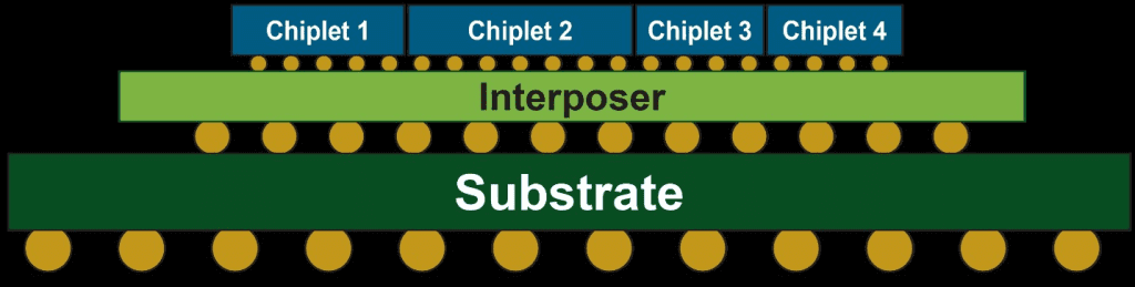
Together, Kyocera’s new capabilities in U.S.-based “OSAT” — Outsourced Semiconductor Assembly and Testing — will enable further adoption of 2.5D and 3D packaging methodologies.
“The U.S. semiconductor industry needs deeper on-shore engineering support during the design, process development, and production of IP-sensitive products,” said Franklin Kim, Vice President of Kyocera’s Semiconductor Components Group in San Diego. “Kyocera can provide this support with state-of-the-art semiconductor package manufacturing and materials to help ensure complex devices are designed for manufacturability at the highest yields — using ceramic, high-density build-up (HDBU) organic, printed wiring board (PWB) organic, or alternative material substrates.”