
Now I know how wafers feel when moving through a fab. Leti in Grenoble, France does so much technology integration that in 2010 it opened a custom-developed people-mover to integrate cleanrooms (“Salles Blanches” in French) it calls a Liaison Blanc-Blanc (LBB) so workers can remain in bunny-suits while moving batches of wafers between buildings. I got to ride the LBB from the 300mm diameter wafer silicon CMOS and 200mm diameter wafer MEMS fabs (Fig.1) along the cement monorail to the more specialized fab spaces for industrial partners and for nanoelectronics start-ups. This was my first time experiencing this world-exclusive ISO 6 (“Class 1000”) mobile cleanroom, and it very nicely moves people in 3 minutes between cleanroom buildings that would otherwise take 30 minutes of de-gowning and walking and re-gowning. In the foreground of Fig.1 is space for a new fab intended for silicon-photonics R&D and pilot fabrication.
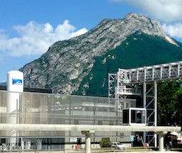
Fig.2 shows the LBB as it passes a Linde gas tower in front of spectacular alpine scenery on the way to Leti’s specialized and start-up fab building. One of Leti’s great strengths is that it does more than just lab-scale R&D, but has invested in all of the tools and facilities to be able to do pilot manufacturing of nanoscale devices. Didier Louis, Leti international communications manager and gracious tour host through the cleanrooms, explained that when working with new materials a pragmatic approach is needed; for example, color coding for wafer transport carriers informs if there is no copper, copper encased by other materials, or exposed copper on wafers therein.
—E.K.