The Intergovernmental Panel on Climate Change (IPCC), the United Nations’ body for assessing the science related to climate change, recently released the latest refinement to its 2006 Guidelines. As part of an effort to tackle climate change, the refined regulations tighten control on new greenhouse gases used in semiconductor manufacturing and increase requirements for reporting and accountability for manufacturers.
“The IPCC has recognised that there is a gap between the amount of greenhouse gas measured in the atmosphere and the amount calculated from the inventory of known sources of emission,” said Prof. Mike Czerniak, Visiting Industrial Professor, Bristol University, and Environmental Solutions Business Development Manager, Edwards. “The gap is of particular concern for gases such as perfluoro compounds (PFCs), which not only have extraordinarily high global warming potentials (GWP) but also extremely long lifetimes in the atmosphere, as long as 50,000 years.”
The IPCC is the scientific organization supporting the United Nations Framework Convention on Climate Change (UNFCCC). Organized by the United Nations and the World Meteorological Organization, the IPCC’s reports provide the scientific underpinnings for the international climate negotiations that led to the 1997 Kyoto Protocol and the 2015 Paris Agreement on climate change. The IPCC reviews the state of the science of climate change every 10-13 years.
“The reason that these refined guidelines have been upgraded was that there was a growing realization that there’s a mismatch between what you measure in the atmosphere, which we refer to as top down and what’s reportedly emitted by humanity which is termed bottom up,” said Prof. Czerniak.
Two new mechanisms for PFC formation during semiconductor manufacturing have been identified and emission factors have been added to the latest IPCC refinement:
1. CF4 formation by reaction of fluorine with hydrocarbon fuel in combustion- based abatement in systems that mix the fuel and process chamber effluent.
2. CF4 formation when cleaning chemical vapor deposition (CVD) chamber deposits.
CF4 is of particular concern because it has an atmospheric life of 50,000 years. “For all intents and purposes, that’s forever,” Czerniak said.
The semiconductor industry took a major step in reducing its carbon footprint years ago by largely replacing perfluorinated gases (PFCs) with less impactful gases, particularly NF3 for processes such as CVD chamber cleaning. “That has massively reduced the carbon footprint of the industry and that was the main way that the industry was able to reach the World Semi- conductor Council targets set for 2010,” Prof. Czerniak said.
With the new IPCC guidelines, semiconductor manufacturers must consider how the NF3 is treated with gas abatement systems, since it’s possible to create CF4 if the NF3 is exposed to the fuel gas. “If you don’t do your abatement in an optimal way, the fluorine that the NF3 is converted into can react with methane or propane fuel gas,” Prof. Czerniak said. “If you do mix the two together and you can actually create some new CF4 that didn’t exist before. For the first time ever, direct accountability required in the form of a data-backed certification from the equipment manufacturer that the reaction is minimized.”
Edwards’ inward-fired combustor avoids the mixing of chamber exhaust and fuel that, in other designs, can lead to the production of PFCs where they did not exist in the original exhaust stream. The lower, more uniform temperature profile of the inward-fired combustor ensures a high destruction removal efficiency (DRE), with low NOx generation. Inward- fired combustors have been standard on Edwards’ abatement systems since the company started developing them in the 1990s. “What we do is we burn the fuel on the combustor pad inside our equipment, so what comes off from the pad and meets up with the fluorine is very, very hot nitrogen and Carbon Dioxide and water vapor,” Prof. Czerniak explained. “It’s the hydrogen in the water vapor that reacts with the fluorine and forms hydrogen fluoride (HF), which is very dilute acid. That’s exactly what we want to happen.” The dilute HF is treated in the fab’s water treatment system, or in some cases repurposed for other industrial applications. In Japan, for example, it is used as part of ceramic making processes.
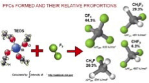
The new IPCC guidelines also point to the possible formation of CF4 during certain semi- conductor processes, such as CVD chamber cleaning. “Say you’ve been growing silicon dioxide using TEOS as your precursor gas,” Prof. Czerniak said. “Each molecule of TEOS has four carbon atoms in it, and that carbon can get left on the walls of the chamber when you’ve done a processing run (Figure 1). When you’re cleaning it with fluorine, it would react with that carbon and start making some CF4. Customers are going to have to start accounting for that and hopefully abating it,” he said.

The semiconductor industry has been relatively proactive with green initiatives such as PFC reduction, but it could potentially be pushed harder in that direction due to the rapid growth of automotive electronics. Consumers purchasing electric cars in an effort to reduce their carbon footprint, for example, may consider the environmental impact of the automotive manufacturing process, including the electronics supply chain.