TECHCET and TechSearch International, Inc. recently announced that the market for Semiconductor Packaging Materials totaled US$26.1 billion in revenues for 2022, and is forecasted to approach US$30 billion in 2027. For 2023, packaging materials are expected to decline about -0.6% given the forecasted slowdown in the overall semiconductor industry. Recovery is expected in the second half of 2023, pointing to growth in 2024 that should increase packaging revenues by 5% that year, as indicated in the recently completed 10th edition of the Global Semiconductor Packaging Materials Outlook (GSPMO).
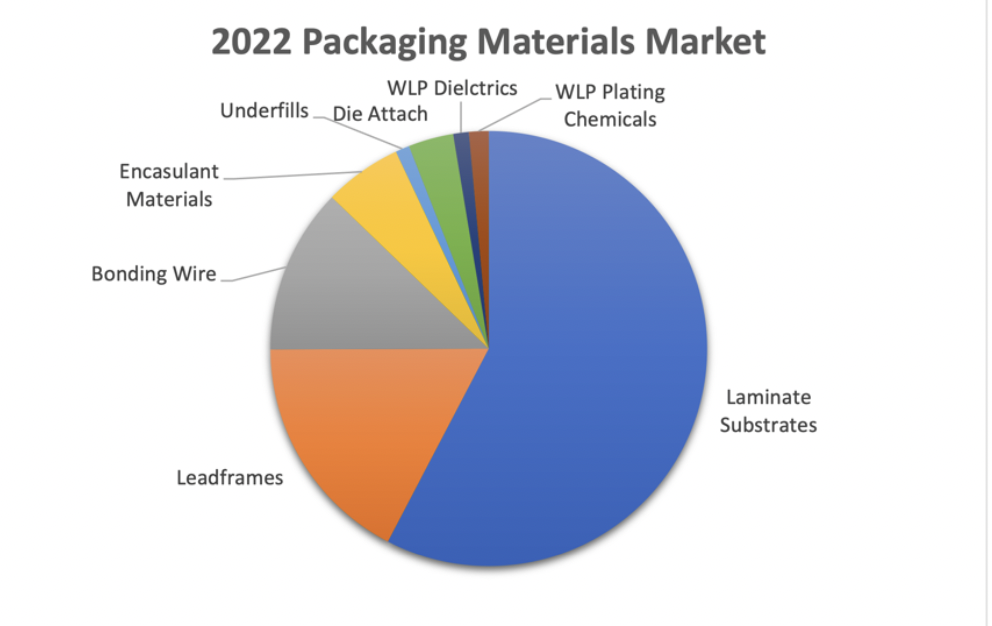
The GSPMO Report is a comprehensive market research study covering key segments of the semiconductor packaging materials market. Available for purchase exclusively through SEMI, this materials report includes a comprehensive look at the market size and growth trends of key packaging materials including substrates, lead frames, bonding wire, encapsulation materials, underfill materials, die attach, solder balls, wafer level package dielectrics, and wafer-level plating chemicals.

Beginning in 2020 through the pandemic, packaging materials experienced strong unit and revenue growth. Changes in end market demand coupled with strained supply chains and logistic constraints boosted pricing for materials across the supply chain. Higher raw material costs, rising energy prices, and soaring logistics costs pushed material suppliers to raise prices, which were passed on to customers. In addition, many material segments were constrained in terms of available production capacity. Being squeezed on rising costs, numerous suppliers limited their capacity related investments. Additionally, as demand rose during the pandemic, supply chain and logistics constrained how rapidly suppliers could expand capacity as available manufacturing equipment was also limited.
The trend in rising material prices was a complete reversal of more than a decade of price reductions, much due to pressure from device makers and OSATs. “Cost-down” became a mantra that limited material suppliers in terms of investments in capacity. These demand driven price increases boosted growth to over 15% in packaging material revenues in 2020, followed by >20% growth in 2021. As long as raw material and energy costs remain high, and the suppliers remain prudent in their capacity expansion plans, current prices are expected to hold.
Wafer-level packaging, flip chip packaging, and heterogeneous integration, including System-in-Package (SIP) form factors are key drivers in new materials development and consumption. For WLP, the largest volume application remains mobile electronics, though other applications are growing, including automotive. Growth in flip chip interconnection remains strong for high performance computing, high frequency communication and other applications, with copper pillar interconnect technology being increasingly used.