Fractilia today announced that it has released the latest version of its Fractilia Automated Measurement Environment (FAME) product to enable semiconductor fabs to control the multi-billion-dollar EUV yield problem of stochastics. The FAME product line uniquely provides highly accurate and precise measurement of stochastics, which are the single largest source of patterning errors at advanced nodes. Armed with Fractilia’s FAME product, fabs can make better decisions faster to solve this new class of yield killers and take back control over their advanced patterning processes, improving their device yields and patterning productivity. This latest release of FAME is built on Fractilia’s proven third-generation Fractilia Inverse Linescan Model (FILM) platform, which is already in use at four of the top five chip manufacturers.
“Stochastics are becoming a major yield problem as semiconductor manufacturing moves further into the EUV production era,” stated G. Dan Hutcheson, vice chair of TechInsights. “Fractilia’s founders,
Ed Charrier and Chris Mack, have been early voices in raising the alarm on stochastics, and are well positioned to help the industry tackle this problem with stochastics control solutions. These two have a proven track record of turning innovative technology into successful commercial products, having developed the PROLITH lithography modeling and data analysis software at FINLE Technologies two decades ago, which was not only well ahead of its time but has remained a mainstay in fab process control to this day. Moreover, FILM has proven to be a very useful tool in pushing EUV out of the lab and into the fab.”

The Stochastics Dilemma: Controlling What You Can’t Measure
Stochastics are random and non-repeating patterning errors, and in EUV processes they can comprise over 50 percent of the total patterning error budget. Fabs need to measure stochastics in order to control them; however, existing methods are unable to measure stochastics with accuracy or precision. At the same time, advanced fabs cannot afford to ignore stochastics. While already a problem at leading-edge 193-nm optical lithography, especially with double and quadruple patterning, stochastics in EUV processes lead to significant yield losses and cost increases.

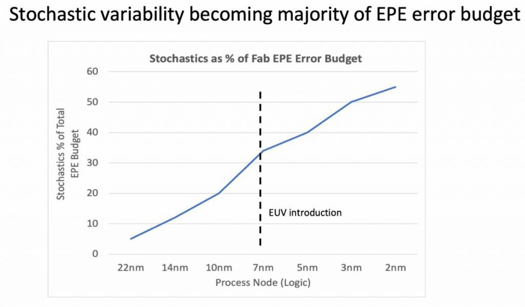
over 50 percent of the total patterning error budget.
According to Chris Mack, CTO of Fractilia, “Stochastics have forced fabs to make a trade-off between yield and productivity. They either need to reduce the throughput of their EUV scanners by increasing exposure dose to avoid yield loss, or bring in an additional EUV scanner to make up for lost productivity. By controlling stochastics, fabs can improve the productivity of the process tools in the fab while increasing their yields. Our FAME product uniquely measures and controls stochastics in the fab with high accuracy and precision, enabling new options and solutions for our customers that otherwise would not be available to them. We’re seeing exponential growth with the number of SEM images measured by customers using our products, making Fractilia the de facto industry standard for stochastics measurements.”

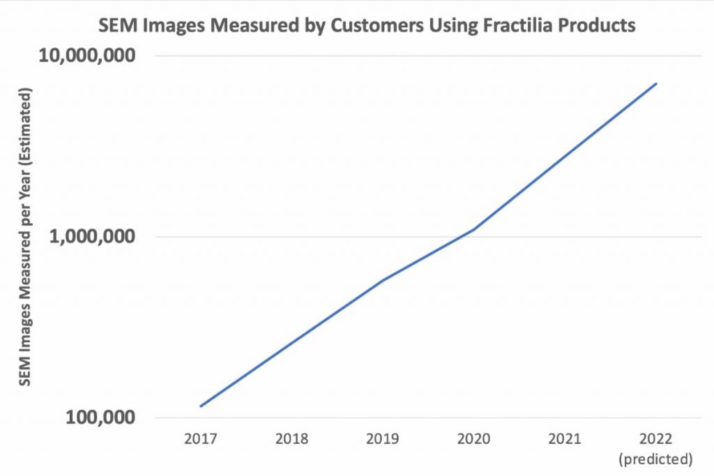
by customers using its products, including FAME.
“Unbiased” Measurements Provide a More Complete Picture on the Wafer
FAME uses a proprietary and unique physics-based SEM modeling and data analysis approach that measures and subtracts the random and systematic errors from SEM images to provide measurements of what is on the wafer rather than what is on the images. These “unbiased” measurements of stochastics enable fab engineers to better understand and solve yield issues.
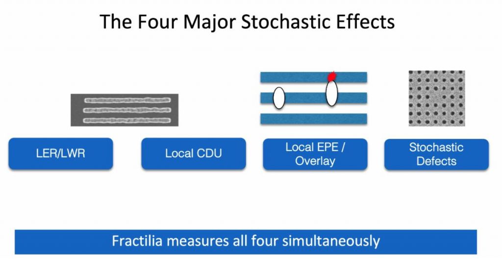
FAME measures all major stochastic effects simultaneously, including line-edge roughness (LER) / linewidth roughness (LWR), local CD uniformity (LCDU), local edge placement error (LEPE), stochastic defects, as well as many more. It provides the highest signal-to-noise edge detection in the industry (up to 5x higher signal-to-noise ratio than other solutions), and extracts more than 30x more data from each SEM image. FAME also works with all SEM tool vendors and all SEM tool models.
New features that come with the latest release of FAME include:
- Accurate and precise measurements even on very high-noise or low-contrast images, which are becoming more important for a variety of use cases such as thin-resist layers for high-NA EUV processes
- First-ever unbiased LCDU measurements for contact holes and pillars
- Unique Probabilistic Process Window capability that uses multiple stochastic metrics, takes measurement uncertainty into account and allows for overlapping of multiple features, resulting in improved scanner control
For process development and engineering analysis applications, Fractilia offers the same high-accuracy and precision measurement performance for stochastics with its MetroLER™ product, which has also been upgraded to the third-generation FILM platform.
More Information
A new video from Fractilia co-founders Ed Charrier and Chris Mack describing how FAME enables fabs to tackle the multi-billion-dollar yield problem of stochastics without compromising yield or productivity can be viewed on the company’s website at www.fractilia.com. Training videos as well as recent conference and technical papers highlighting Fractilia’s solutions for measuring and controlling stochastics can be found at the Fractilia Academy at https://www.fractilia.com/public-academy/.