
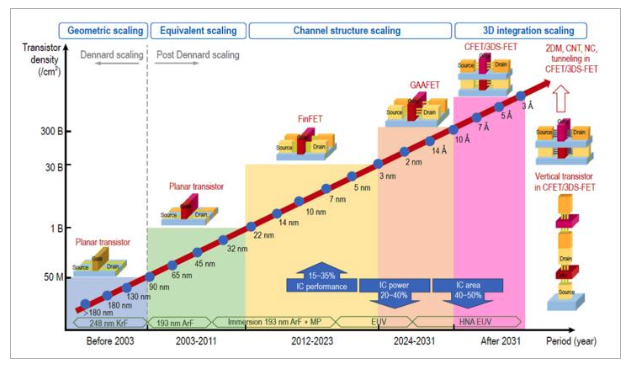
This review is summarized by the research team led by Prof. Huaxiang Yin (Institute of Microelectronics of Chinese Academy of Sciences). They systemically reviewed the development history of Si-based metal-oxide-semiconductor field-effect-transistors (MOSFETs) including the theory update, new materials introduction, key processes breakthrough, especially on device structure innovations for the development of advanced integrated circuits (ICs) in the past twenty years.
The structure of the Si-based transistors would be changed from the fin field-effect transistor (FinFET) to the cutting-edge Stacked NanoSheet/NanoWire Gate-All-Around FETs (GAAFETs) at 3 nm node. Therefore, they introduce up-to-date GAAFET integration process method and the recent technical progress in research institutions and IC industries. Furthermore, the key challenges in fabricating the GAAFETs are illustrated detailly, including high-quality GeSi/Si superlattice periodic epitaxy, channel release, inner spacer module, SD-selective epitaxial defects, parasitic sub-fin channel leakage, and HKMG filling, low hole mobility in the (100) orientation, high voltage (HV) and input/output (IO) integration, and high parasitic capacitance during AC operation. Some innovations in GAA devices, e.g. Forksheet FETs,Tree FET, Fishbone FET,CombFET are also introduced by the authors.
Beyond GAAFETs, CFETs also known as 3D Stacked FETs (3DS-FETs) are showing promise for scaling toward the 1 nm node. The authors introduced two CFET integration process method: sequential and monolithic CFETs. They analyzed the differences between these two kinds of CFET structures, respective advantages, and the challenges in the fabrication process. In addition, the top layers using new channel materials including CNTs, 2DMs, and AOSs with low-temperature processing characteristics, are becoming trend of future 3D stacking technologies. Beyond device structure and process breakthroughs, CFETs require a full DTCO or STCO to enable the construction of transistors, circuits and even systems at various levels for higher PPA gain.
Except for horizontal and lateral conductance channels, the new paths vertical GAAFETs (VGAAFET) have also been summarized, including vertical devices W. and W.O. self-aligned gates for 3DS-FETs. There are great advantages in continuous reduction in their contacted gate pitch (CGP), the SDC and SRAM cell areas. Additionally, VGAAFETs also offer new opportunities for 3D integration in dynamic RAM (DRAM) and NOR-type memory application.
Eventually, they summarized the critical challenges, such as precise process control at atomic level, incredible heat dissipation and augmented parasitic capacitance/resistance during high-speed circuit operation need to be solved for vertical transistor 3D stacking application into mainstream IC industry. They also provide insights into the future development pathways integrating transistor 3D stacking with new theory transistor like tunneling, negative capacitance, and quantum devices in innovative monolithic 3D chip and system. The review has a significant guidance for advanced IC manufacturing, modeling, and design area for 3 nm node and beyond.