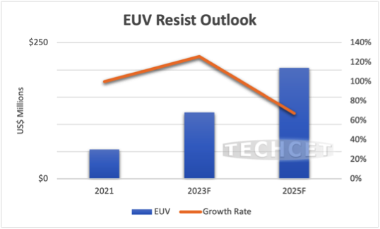
TECHCET—the electronic materials advisory firm providing business and technology information— reveals that Extreme Ultraviolet (EUV) applications have resulted in several photoresist technology platforms including Metal Oxide photoresists, Dry Deposited photoresist, and Multitrigger photoresists, all driven by the process technologies required in advanced chip manufacturing. Combined, these resist platforms will up the market to reach more than $200M by 2025, as highlighted in the recently released Critical Materials CMR™ Market Report on photolithography.

Metal Oxide photoresists have a high etch resistance that can eliminate additional layers required above the resist. Dry deposited photoresist offers the opportunity to eliminate liquid development and deposition, thus decreasing ancillary consumption and lowering waste requirements. Multitrigger Photoresists enable the continued use of lower exposure energy, making it useful in multiple exposure regimes while demonstrating improvements over the photoresist of record.
With EUV in high-volume manufacturing, the photoresists and related ancillary have firmly ‘arrived’ and are now officially being used at multiple chip makers. EUV photoresist will grow rapidly as new logic nodes continue to be introduced. Additionally, advanced DRAM enters production with EUV and as scanners are placed into production. In addition to photoresists, EUV is ushering in a number of changes such as scanners optics and 3D patterning techniques.
“Photolithography materials are critical in semiconductor manufacturing and are an important component in lithographic processing as semiconductor fab costs are rising at the leading-edge. Thus, materials and process innovation, as in the example of EUV, will ramp,” states Lita Shon-Roy, CEO at TECHCET.
These newer materials, are giving a boost to the lithography materials market, and are expected to grow 5X over the next 3-4 years with the advancement in fine line-width device manufacturing.