By PETER GILLESPIE, VP and GM, Semiconductor Products, Advanced Energy Industries, Inc., Milpitas, CA
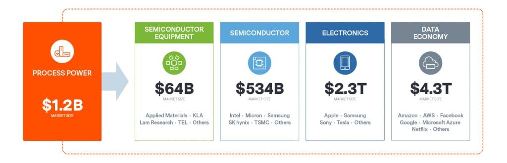
The semiconductor processing market has always been dynamic, but today the industry is experiencing unprecedented growth and change with the rise of the data economy and the 4th Industrial Revolution. According to industry forecasts, the global semiconductor manufacturing equipment market is projected to reach over $64 billion in 2020 [1], supporting the $534 billion semiconductor industry [2] that feeds the $2.3 trillion electronics market [3] and enables the $4.3 trillion information and communication technology market [4], the backbone of the data economy.
Sometimes overlooked and under-appreciated, critical subsystems (CSubs) are the highly specialized subsystems such as lasers, optics, robotics and process power that are increasingly being tapped by semiconductor fabrication equipment manufacturers to advance semiconductor processing.
At the forefront of CSubs, process power is one of the most critically enabling technologies used for etch, deposition, inspection, implantation and electron beam (e-beam) inspection. Process Power has become more crucial as devices shrink to sub 14 nm nodes because it is intimately tied to the wafer process itself and lives at the very heart of device feature fabrication. Without radio frequency (RF) process power, there would be no plasma, no chips, no servers, no data centers, no data economy, and thus, no Google, Amazon, or Facebook.
Formerly somewhat hidden from view, process power is growing at a rate even faster than the semiconductor equipment industry itself, with a Served Available Market (SAM) compound annual growth rate (CAGR) of 11.9% (2014-2019), which is well above the wafer fab equipment (WFE) CAGR of 7.3% [5]. Now a $1.2 billion market, process power [6] is outpacing WFE because of ever-evolving technology requirements and the increasingly sophisticated and enabling capabilities it provides (Figure 1).

With planar devices shrinks (Dennard Scaling) falling short in extending Moore’s Law, the race to find alternatives has resulted in new transistor architectures, 3D structures and processing, new materials and more—all driving broad and deep changes, the elemental nature of which are fundamentally altering requirements and, in turn, transforming the role and significance of process power.
While RF process power has always played a key role in creating plasma for thin film etch and deposition processes, simply creating plasma is no longer adequate. Now, process power is the heartbeat of semiconductor plasma processes with its complex ultra-fast pulsing, microsecond response times, multiple frequencies, extreme duty cycles, and amazing agility to keep plasmas ignited through wildly dynamic pressure, flow and chemistry changes.
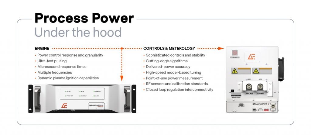
In fact, process power is now providing the most critical knobs enabling plasma processing to deliver increasingly complex three-dimensional features. No longer “dumb black boxes,” RF power generators and matching networks are complex systems with sophisticated controls, cutting-edge algorithms and power control: response, accuracy and granularity that would have been unthinkable even just ten years ago (Figure 2).

At the same time the demands on process power have transformed, the level of technology risk has risen, with device manufacturers making bigger bets in shorter timeframes. As these risks move down the supply chain, they become intensified and amplified.
For instance, a memory integrated circuit (IC) manufacturer may identify a new process application need. To ensure their market success, they must implement at their next product insertion within a four to six-month window. Semiconductor tool manufacturers are required to quickly react, often without having complete process information or insight to fully characterize the application. Despite this, tool makers must move forward beyond initial modeling to semi-empirical optimization within a time span as short as two to four months. This fast-paced tool optimization may require customized RF power generators and matching networks to be ready in as little as one to two months. From there, suppliers and customers are learning together and iterating quickly, knowing this intensive parallel/serial development is playing out where the win/loss stakes couldn’t be higher.
New architecture and materials challenges are resulting in the need to develop more and more complex process power products in those shorter timeframes. Unlike the past where there were few RF frequencies and power levels in use, now 400 kHz, 1 MHz, 2 MHz, 13 MHz, 27 MHz, 40 MHz and 60 MHz at wide-ranging power levels are commonly used.
There is no longer a one-size-fits-all process power approach. RF power must be tailored to a growing fragmentation of applications. This power customization is increasingly the new fundamental enabler for forming advanced features in semi devices. With power content per tool increasing, multiple RF frequencies (dual or triple frequencies into a single matching network, for instance) and advanced capabilities including pulsing and fast tuning drive continuous innovation, as it is increasingly necessary to meet sub 10 nm technology nodes.
As 3D IC layer counts climb from 24, 48, 96 128, and 256 and even 512 or more looking forward, deeper, more narrow 3D features are drivers increasing demands on RF process power. Simply adding more power is not enough. Extending power alone is a linear solution to an exponential problem. Increasing power eventually becomes untenable; future stacks may need etch tools with 600 kW or RF power—or even up to 1MW peak per tool – if current trends were extrapolated.
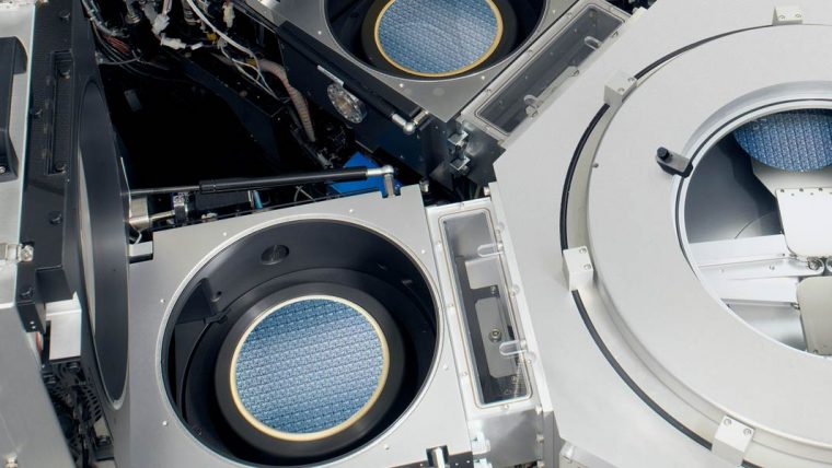
Add to that, the jeopardy of increasingly inefficient power transfer to the plasma and the extraordinary thermal challenges to the plasma reactors, taking a brute force approach to “scale” RF process power will likely not be enough to power future device structures. The emerging novel semiconductor processes that RF process power is helping to create is an area where innovation is bringing fresh solutions and exciting new possibilities both today and in the future (Figure 3).

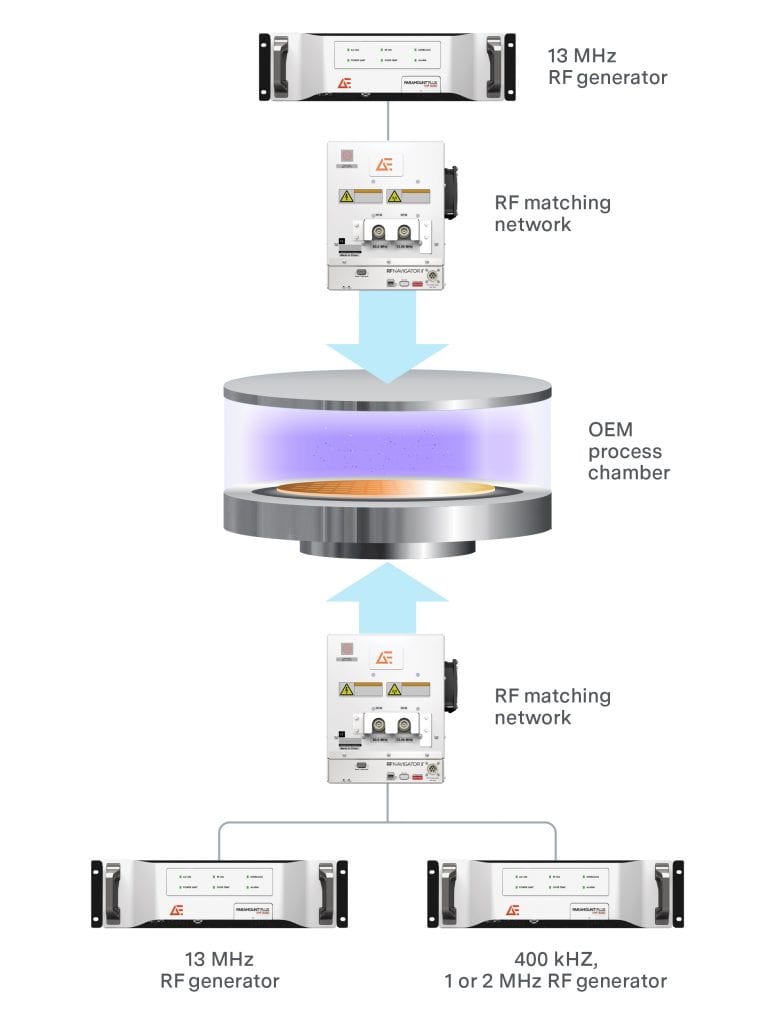
Taken altogether, the role of process power has stepped out of the shadows. RF process power (Figure 4) is enabling processes in semiconductor etch, deposition, ion implantation and inspection (e-beam) in fundamentally new ways. No longer seen as “dumb black boxes,” RF process power now provides precise control for plasma creation and gas dissociation, accurately operates at multiple frequencies, drives energy through complex electrostatic chucks and delivers directionality and control to sub-10 nanometer features–often while pulsing to ensure device feature fidelity, as will be discussed in an upcoming article.

In part two of this series, the following questions will be addressed and answered accordingly:
- What’s working?
- What’s not working?
- Why multi-frequency RF?
- Why pulsing?
- Why are matching network requirements going up by 10X or more?
- What’s next?
Considering that process power is now at the backbone of the semiconductor manufacturing industry, it will be crucial to look at the past, present and future in order to understand how it has become the new enabler, or as some say, “the new lithography.” With ICs now a part of nearly every product in consumer, entertainment, manufacturing, computing, transportation and many other markets, our industry is faced with a much wider range of applications and with process development moving faster than ever. In a highly competitive market where there are a small number of powerhouse players, CSubs—and particularly process power—are a key crucible of innovation that is enabling new leaps in semiconductor processing.
References
1. Source: SEMI.org
2. Source: VLSI Research
3. Source: VLSI Research
4. Source: IDC
5. Source: VLSI Research
6. Source: VLSI and Advanced Energy Industries estimates