Author’s Note: This is the last in a series of 10 installments that explore certain fundamental truths about process control—defect inspection and metrology—for the semiconductor industry. Each article introduces one of the 10 fundamental truths and highlights its implications. Within this article we will use the term inspection to imply either defect inspection or a parametric measurement such as film thickness or critical dimension (CD).
In the eighth installment1 in this series, “The Tyranny of Numbers,” we discussed the trend of increasing process steps—the number of steps is expected to double between the 20nm and 10nm nodes—and the impact that those additional steps will have on final yield. In addition to impacting yield, the increased complexity of the process flow will also increase production costs and cycle time. As these trends unfold, managing costs and cycle time will become increasingly important to fab operations.
The tenth fundamental truth of process control for the semiconductor IC industry is:
Adding Process Control Reduces Production Costs and Cycle Time
Instrumental to having an efficient, low-cost fab is the ability to collect meaningful information about the process in a timely fashion. Process control tools (metrology and inspection) are the eyes and ears of the fab in that they provide insight into what’s working and what’s not: they are an investment in “process information.” In a 2007 paper2 the National Institute of Standards and Technology (NIST) estimated that the average return on investment for metrology alone was 300 percent.
Previous articles in this series have illustrated how process control can reduce costs by reducing the scrap and raw material costs associated with lost yield and reliability3 failures. Similarly, improving yield reduces the environmental footprint of fab operations per good die out.4 In this article, we will examine two other elements of cost reduction and factory efficiency enabled by process control:
Process equipment re-use from node-to-node
Improved net cycle time
Equipment Re-Use
The single biggest component of cost in a modern fab is capital depreciation. It can vary from company to company, but typically wafer fab capital equipment is depreciated at 20 percent per year over the course of five years. If you can extend the life of a piece of equipment beyond the point where it is fully depreciated you are essentially getting that tool for free. If you can find a way to re-use an entire group of process tools (scanners, etchers, etc.) the savings could easily be measured in tens or even hundreds of millions of dollars.
Ultimately, a process tool must meet the technical specifications that are demanded by the manufacturing process in which it is used. However, in cases where the tool’s capability is marginal, its lifetime can be extended by closer monitoring—using existing metrology or inspection tools to keep the tool operating within the required process specifications. Performing more frequent process tool qualifications can help improve matching and ensure that a tool does not drift out of spec. For stable feed-back and feed-forward schemes, having more in-line inspections provides better averaging and allows for better control of the actual process. In these situations, process control is helping to extend the life of existing process tools—adding process control in this context can actually save money.
The Process Capability Index (Cpk) is a metric that measures how well the natural variation of a process fits within the spec limits. For a centered process with a symmetric distribution the Cpk is given by equation 1,
Cpk = (USL – LSL) / 6σ Eq. 1
where USL and LSL are the upper and lower spec limits respectively and σ is the standard deviation of the process. If the Cpk value is greater than one, the process is considered capable. Cpk values less than one indicate that the process is not capable.
Consider an etch process step where the Cpk of the CD measurement is exactly equal to one (i.e., the step is marginally capable in that the upper and lower spec limits are both three standard deviations from the mean). The marginal capability could be the fault of the previous photo step, the etch step or both. Either way it is an expensive proposition to upgrade either tool set to improve the Cpk—the capability —of the process.
Often the capability of the process can be improved by implementing a data feed-forward scheme—using additional metrology to fully characterize the process at one step (e.g., photo) and then feeding that information forward to adjust parameters at etch to effectively customize the process conditions for each lot or wafer. Figure 1 below shows an example Statistical Process Control (SPC) chart of the after-etch CD with and without feed-forward.

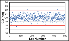

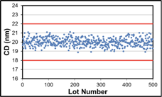
Figure 1. Left: SPC Chart of etch CD without feed forward (Cpk=1.0). Right: SPC Chart of etch CD with feed forward (Cpk=1.3)
Feed-back and feed-forward schemes can be used to extend the useful lifetime of process tools by effectively increasing the process window in which they operate. CD measurements that are slightly off target at photo can be brought back on target by using that information to adjust the etch bias at the etch process step.
Cycle Time
Cycle time is another very important production metric. We will give a more detailed account of cycle time in an upcoming paper but would like to touch briefly on the counter-intuitive relationship between cycle time and process control.
Any source of variability that prevents lots from moving through the fab in lock-step fashion will increase the cycle time. Adding inspection steps will add cycle time to those lots that get inspected but due to sampling (not every lot gets inspected) it will have a much smaller impact on the average. When an excursion does occur, comparatively few process tools will have to be put down (because the inspection points are closer together) and the module owner will be able to isolate the problem much sooner. The total disruption to the fab (the variability) will be reduced and the cycle time of all lots will be improved. This counter-intuitive concept has been demonstrated by several fabs that have both added inspection steps and reduced cycle time simultaneously.
To summarize, adding process control steps contribute to fab efficiency on several levels (figure 2): increasing baseline yield, extending the useful life of existing process tools, limiting the duration of excursions, and reducing cycle time.

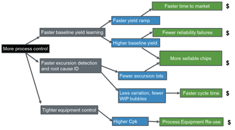
Figure 2. The cascading benefits of process control.
As we conclude this series on the 10 fundamental truths of process control1,3,5-11, we thank you for reading. We hope that these articles have provided deeper insight into the value of process control and the base knowledge for successful implementation of process control in IC fabrication. We look forward to exploring additional aspects of process control in future Process Watch articles throughout the coming months.
References:
Process Watch: Increasing Process Steps and the Tyranny of Numbers, Solid State Technology, July 2015
“Economic Impact of Measurement in the Semiconductor Industry,” Planning Report 07-2, National Institute of Standards and Technology, U.S. Department of Commerce, December 2007.
Process Watch: The Most Expensive Defect- Part 2, Solid State Technology, July 2015.
Reducing Environmental Impact with Yield Management, Chip Design, July 2012.
Process Watch: You Can’t Fix What You Can’t Find, Solid State Technology, July 2014
Process Watch: Sampling Matters, Semiconductor Manufacturing and Design, September 2014
Process Watch: The Most Expensive Defect, Solid State Technology, December 2014
Process Watch: Fab Managers Don’t Like Surprises, Solid State Technology, December 2014
Process Watch: Know Your Enemy, Solid State Technology, March 2015
Process Watch: Time is The Enemy of Profitability, Solid State Technology, May 2015
Process Watch: Risky Business, Solid State Technology, September 2015.
About the authors:
Dr. David W. Price is a Senior Director at KLA-Tencor Corp. Dr. Douglas Sutherland is a Principal Scientist at KLA-Tencor Corp. Over the last 10 years, Drs. Price and Sutherland have worked directly with more than 50 semiconductor IC manufacturers to help them optimize their overall inspection strategy to achieve the lowest total cost. This series of articles attempts to summarize some of the universal lessons they have observed through these engagements.