How to keep semiconductor fabs supplied with critical materials despite a pandemic and trade wars was discussed by >250 industry experts gathered in virtual space October 21-22 during the 5th annual Critical Materials Council (CMC) Conference. CMC Fab Members and Associate Supplier Members were joined by leading industry analysts, educators, and investors in discussing business and technology trends in the value-chain for advanced packaging, logic, and memory. The “after-hours” virtual conversations will continue through December 11th using the conference app and website, and new people can join in through November 16th.
“There were a lot good topics especially on materials challenges for leading edge technology and heterogeneous integration, global issues on material supplies, and emerging materials development,” commented Dr. Lihong Cao, Director of Engineering and Technical Marketing at ASE, and Session 4 presenter.
This was the first year that a new conference session was dedicated to Advanced Packaging of Heterogeneous Integration using chips from different fabs. Dr. Lauren Link of Intel discussed the need to find ways to integrate more front-end fabrication materials into packaging. The challenge is how to do so in a cost-effective manner, without over-specifying materials and process requirements as shown in the screen-capture (Figure).

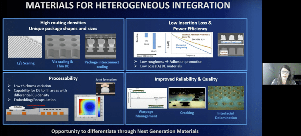
While materials revolutions are happening in advanced packaging, materials evolutions are also essential to improve reliability and quality. Dr. Alejo Lifschitz of DuPont showed how the clever addition of a new “Grain Refiner” additive to the company’s chemistry blend allows for electro-chemical deposition (ECD) of copper (Cu) lines that have reliability engineered into the micro-structure. As deposited, the new Cu grains for the package Re-Distribution Layer (RDL) are <0.2 micron in size with >93% in maximum density highly-twinned <111> crystallographic orientation. This makes reflowed Cu RDL lines that are inherently more resistant to corrosion and cracking when subjected to chemical and mechanical stresses in the real world.
Advanced Logic: finFETs and NanoSheets
Fin-based Field Effect Transistors (finFET) in the most minimally-scaled logic chips will soon be replaced with Horizontal Nano-Sheets (HNS) to improve device performance. HNS are Gate All-Around (GAA) CMOS FETs that reduce power-consumption while allowing for simple patterning of different gate-widths so that designers can optimize power:performance trade-offs within the IC layout. However, both evolutionary and revolutionary new manufacturing processes will be needed for commercial fabrication of HNS logic ICs.
The best example of a revolutionary new process that is needed to make HNS ICs is that of the epitaxial (Epi) growth of the layers to make the transistor channels. Pamela Fischer of ASM in presenting on, “Materials Evolution and Challenges in ALD/Epi FEOL,” explained that when growing alternating Epi layers the interface transition thickness directly determines final device performance. The company’s latest Epi tool allows for alternating ~10nm thick layers of silicon (Si) and silicon-germanium (SiGe) to be grown with extremely sharp transitions of just ~0.5nm. This means that the transition happens in ~2 atomic layers of silicon!
Advanced Memory Materials
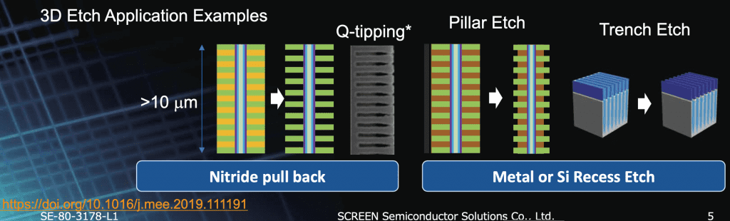
3D device fabrication issues in logic fabs pale in comparison to the ongoing challenges with finding integrated process flows for 3D-NAND memory chips, which currently stack ~100-device-layers and will soon aim for ~200-device-layers on each silicon wafer. Dr. Ian J. Brown, VP Engineering for SCREEN Semiconductor Solutions, showed how “Wet Etching in the 3D Era” has evolved to enable 3D device structures for both logic and memory (Figure). Tools are becoming more sophisticated to allow for chemical blending on-site in the fab, which allows for cost-effective use of more complex chemistry sets. “Digital Wet Etch” (DWE) is a 2-step process similar to Atomic-Layer Etch (ALE), where a first chemistry oxidizes the surface of a metal such as copper (Cu) or cobalt (Co) following which a second chemistry selectively removes just the metal-oxide layer.

Shaun Miller, Director of Global Front End Materials Procurement for Micron Technology, showed why independent regional supply-chains can create, “Material Challenges in Leading-Edge Memory Manufacturing.” For example, differences in supplier infrastructures between the U.S. and Taiwan have led to different levels of metallic and particle impurities in wet chemicals such as sulfuric-acid and hydrogen peroxide, with Taiwan leading in purity at present. Micron is using analytics and “big data” to collaborate on a deeper level with suppliers.
In follow-on conversation, Terry Francis, TECHCET Sr. Analyst who also presented at the conference, explained how hydro-fluoric acid (HF) supply in North America is likely to change in the near term. The raw material supply is changing from mined fluorspar mineral to chemically-engineered fluorosilicate- acid (FSA), since the latter is in surplus as a byproduct of phosphate-based fertilizer production. While electronics manufacturing consumes at most 1% of industrial demand, there is insufficient volume to sustain a supply-chain independent of that for general industry. Such a change in upstream material source would inherently change the trace contaminants in the final downstream HF, which could trigger random yield losses in advanced IC fabs unless materials are carefully re-qualified.
Post-event registration is open until November 16th, so click through to access recordings of presentations and discussions, connect with attendees, and engage in follow-up Q&A!