By Emily Newton, a tech journalist and the Editor-in-Chief of Revolutionized.
There’s a growing interest in creating flexible circuits to increase the possibilities for new electronics. Some of the related devices could include:
- Medical monitors
- Fitness trackers
- Smart clothing
- Foldable smartphones
Many of the obstacles associated with this work relate to the challenges of achieving the kind of miniaturization required for high-performance electronics. However, researchers at Stanford University recently made significant advances in this area due to a pioneering manufacturing breakthrough. Here’s what you need to know about this achievement and how it could change the industry moving forward.
Researchers progress with flexible and wearable electronics
The manufacturing technique invented by the Stanford team makes it possible to create flexible and atomically thin transistors that are several times smaller than previous efforts. These creations are less than 100 nanometers long. The group calls them “flexitronics.”
Previous research indicated that two-dimensional semiconductors are especially suitable candidates for flexible electronics, at least compared to alternatives such as conventional silicon or organic options. That’s largely because the semiconductors retain their fantastic electrical and mechanical properties at the nanoscale.
These are also high-performance transistors. In the context of this study, that descriptor means they can tolerate high electrical currents while operating at low voltage. Such characteristics make them ideal for applications that require low power consumption levels.

Looking ahead with a layering technique
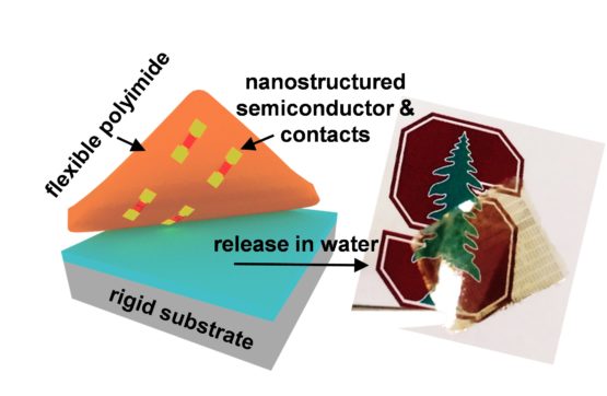
The main engineering challenge to date when making incredibly thin devices was the heat intensity required during the process. It was so high that the flexible plastic substrates would melt and break down during the manufacturing process. However, Eric Pop, a Stanford electrical engineering professor, and Alwin Daus, a postdoctoral scholar, came up with a new layer-based process. It required starting with a nonflexible base substrate made from glass-coated silicon.
They then formed an anatomically thin film of a molybdenum disulfide (MoS2) two-dimensional semiconductor featuring an overlay of small, nano-patterned gold electrodes. Those metal contacts help dissipate and spread the heat generated by transistors during operation. This manufacturing approach allows using advanced patterning techniques on the nanoscale transistor dimensions while remaining on the traditional silicon substrate. The results give a resolution that was previously out of reach with flexible plastic substrates.
In the abstract of the research paper about this achievement, the researchers wrote, “Despite the low thermal conductivity of the flexible substrate, we find that heat spreading through the metal gate and contacts is essential to reach such high current densities.”
The researchers grew a MoS2 film layer by layer with a technique called chemical vapor deposition. It produces a coating with thermally induced chemical reactions occurring at a heated substrate’s surface due to gaseous reagents. This process creates a film measuring only three atoms thick. However, it requires working with temperatures of over 1,500 F to work.
If the team had started with a flexible polyimide substrate, it would have lost its shape due to excessive heat at around 680 F and decomposed as the temperature elevated. The key to success involves using rigid silicon as the substrate for patterning and forming these vital parts and then letting them cool.
Exciting opportunities on the horizon
After completing the patterning and formation of the parts, immersion in deionized water makes the whole device stack peel back. It can then be fully transferred to the flexible substrate made from polyimide. There are a few more fabrication steps afterward. Even so, the process enables making flexible transistors that can demonstrate high performance several times better than any previous effort characterized by atomically thin semiconductors.
In the abstract of their research paper about the method, the team summarized their new approach to these flexible field-effect transistors (FETs). They explained, “… We report flexible nanoscale FETs based on 2D semiconductors; these are fabricated by transferring chemical-vapor-deposited transition metal dichalcogenides from rigid growth substrates together with nano-patterned metal contacts, using a polyimide film, which becomes the flexible substrate after release.”
The researchers also clarified that it’s possible to build entire circuits before moving them to the flexible substrate. However, they said it was easier to only add a few layers and transfer them before moving ahead with the final steps. That’s because they realized that doing everything before the transfer caused preventable challenges with subsequent layers.
The outcomes are undoubtedly impressive. Pop confirmed, “In the end, the entire structure is just 5 microns thick, including the flexible polyimide. That’s about 10 times thinner than a human hair.”
People not involved with the research think the remarkable thinness could lead to advancements in electronic skin, particularly since it must be virtually imperceptible to become viable. However, for possibilities like that to become feasible, the team must figure out how to scale up their operations to make them commercial-ready.
What’s next for these flexible circuits?
Pop and Daus completed their prototype and submitted a patent application for their work. They’re now focused on refining the technique and considering what future possibilities exist. The pair have also built these transistors with molybdenum diselenide (MoSe2) and tungsten diselenide (WSe2) semiconductors to show the versatility of this manufacturing approach.
Energy harvesting technologies are especially exciting potential applications for flexible circuits. For example, options that work with piezoelectric energy could gather power as people move or breathe. Statistics show that the energy harvesting market will reach $2.6 billion by 2024.
Daus is also eager to experiment with the possibilities of embedding radio circuits into these flexitronics. Success in that regard could enable wireless communications that would be particularly advantageous for devices implanted into the human body or wires built into Internet of Things (IoT) gadgets.
If this manufacturing technology becomes widespread, it could help countries like the United States regain some former competitiveness in the microelectronics fabrication industry. Recent data showed that the U.S. only has a 12% share of the chip manufacturing market compared to an 85% segment of the chip design software segment.
Other advancements in flexible electronics
The work carried out by the Stanford University team is among other notable progress made elsewhere that could change how people design and manufacture products that feature flexitronics. For example, researchers developed a better way to apply conductive ink when adding flexible electronic circuits to surfaces.
The conventional way involves depositing the ink using specialized devices. However, those applicators can get clogged. Researchers solved the problem by creating pens that put the ink onto smooth or irregular surfaces without getting stopped up.
In another instance, researchers worked on printing flexible energy storage devices, including flexible supercapacitors (FSC). Those have a high power density, as well as fast charge and discharge rates. The typical manufacturing process for an FSC involves printing functional inks onto traditional organic and inorganic electrode materials on flexible substrates.
This new research uncovered two principles to follow when selecting optimal functional inks. First, the researchers determined it’s best to choose inks with fewer nonessential additives, an appropriate dispersion of electrode materials and good conductive binders. Moreover, the ink is most likely to give high-quality prints if it has a suitable viscosity and a good rheology property.
These findings should aid future researchers and manufacturers as they aim to make better printable ink choices. The results could influence products ranging from solar cells to flexible display screens.
Are flexitronics the future?
It’s still unclear when the achievements from Stanford and elsewhere could appear in mainstream flexible electronics. However, it makes sense that flexitronics could become even more in demand soon.
For example, health care practitioners have already noticed the payoffs of monitoring people with minimally invasive devices. If the gadgets get thinner, they become more comfortable and could be good picks for infant patients or even veterinary applications. Although it may be a while before flexitronics become commonplace, it’s easy to see their abundant potential.


Emily Newton is a tech journalist and the Editor-in-Chief of Revolutionized.