Contributed by Dick James, Fellow Emeritus, TechInsights
The VLSI Symposia are coming up on June 12 – 17, at the Hilton Hawaiian Village in Honolulu, and recently their media associates released the tipsheet describing some of the upcoming papers. The detailed program is available here.
Of the eighteen papers Samsung is presenting at the conference, three are noted in the tipsheet. In the DRAM Memory category, Samsung are up first in the 15th session (C15-1), with “A 16 GB 1024 GB/s HBM3 DRAM with On-Die Error Control”.
Samsung’s third generation of 10-nm DRAM (1z) has improved performance with greater system reliability, availability, and serviceability (RAS), targeting automotive, industrial, and data center applications.
To do this, they use a new scheme for on-die error code correction (ECC) which can correct for a 16bit word error and 2 single-bit errors simultaneously, and have incorporated it in their new version of “High Bandwidth Memory-3” (HBM3) DRAM.

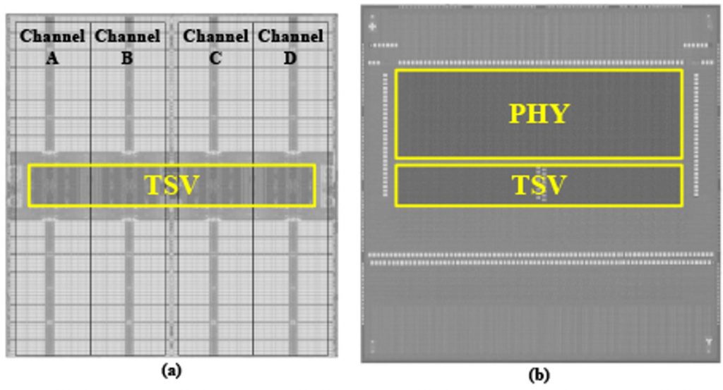
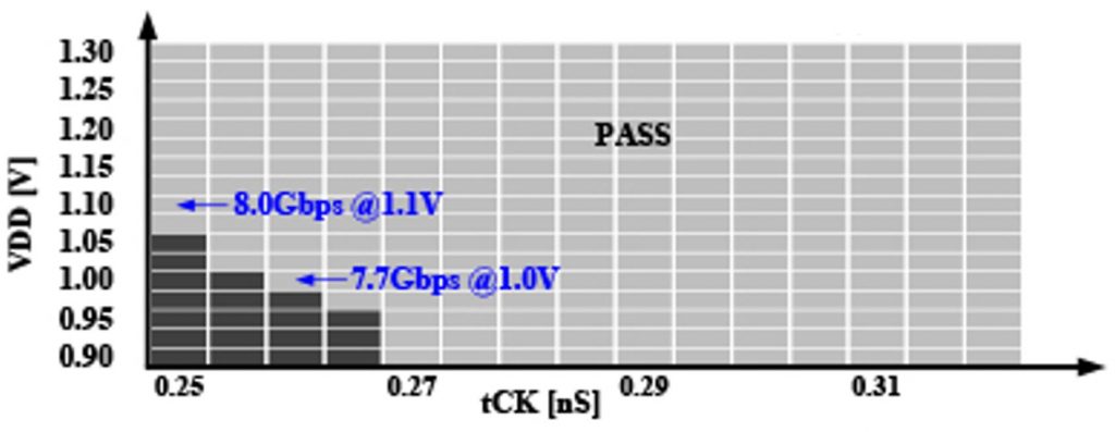
Performing the correction locally on each individual DRAM die, instead of having to access other dies in the stack, reduces latency and increases the pin data rate from the previous generation’s 5 Gb/s/pin to 8.0 Gb/s/pin, giving a total memory bandwidth of 1024 GB/s per memory cube. This was demonstrated in a 16 GB DRAM module.

The Samsung 3-nm gate all around FET (GAAFET) technology gets an airing in paper C21-4 “A 3nm GAAFET Analog Assisted Digital LDO with High Current Density for Dynamic Voltage Scaling Mobile Applications”, so they are clearly beyond making SRAM test wafers in this process.
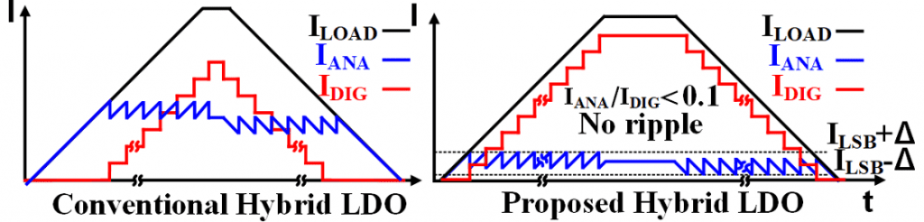
Here analog assisted digital LDOs are discussed, which provide high current density power delivery. The design has active supply noise cancellation and fast transient load detection of CPU cores.

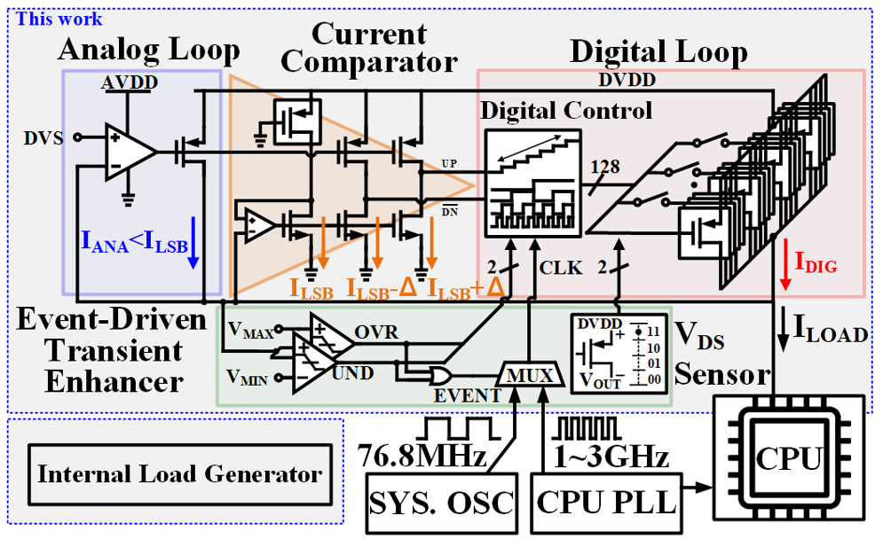
This hybrid LDO design achieves accurate regulation over <1 mA to 1.4 A load range, and only 38mV supply droop for a 1 A dynamic load in 1 ns.

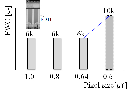
In the technology sessions, we have a paper on “A 0.6μm Small Pixel for High Resolution CMOS Image Sensor with Full Well Capacity of 10,000e- by Dual Vertical Transfer Gate Technology” (Paper T8-4).
Samsung have developed a prototype 200 Mp image sensor using 0.6μm pixels with a full well capacity (FWC) of 10,000 e- using a dual vertical transfer gate (D-VTG) technology. Compared to single vertical transfer gate, the FWC of the D-VTG increases by 60%, and improves the transfer properties due to the improved controllability of transfer gate voltage.

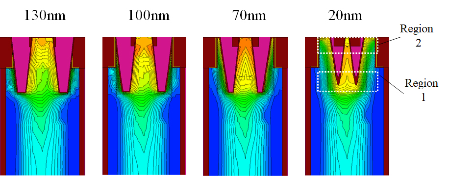
The photo-electron transfer is optimized by adjusting the gap, depth, and taper slope of the VTGs, as shown below.

There are fifteen more Samsung papers at the conference:
C10-1 A 12-bit 8GS/s RF Sampling DAC with Code-Dependent Nonlinearity Compensation and Intersegmental Current-Mismatch Calibration in 5-nm FinFET
C10-3 A 0.56mW 63.6dB SNDR 250MS/s SAR ADC in 8-nm FinFET
C11-5 Fully Integrated 2×2 MIMO Real Simultaneous Dual Band WiFi CMOS Power Amplifiers With a Single Inductor Multiple Output Supply Modulation Technique
C14-2 High Efficiency 29-/38-GHz Hybrid Transceiver Front-Ends Utilizing Si CMOS and GaAs HEMT for 5G NR Millimeter-Wave Mobile Applications
C15-2 A 32 Mb Embedded Flash Memory based on 28 nm with the best Cell Efficiency and Robust Design achievement featuring 13.48 Mb/mm2 at 0.85 V
C17-1 A 40-Gb/s/pin Low-Voltage POD Single-Ended PAM-4 Transceiver with Timing Calibrated Resetless Slicer and Bidirectional T-Coil for GDDR7 Application
C16-3 An Automotive ASIL-D Safety Mechanism in ADC and DAC for Communication Application
C18-5 Palm-sized LiDAR module with III/V-on-Si optical phased array
C19-3 A 12-bit 10GS/s 16-Channel Time-Interleaved ADC with a Digital Processing Timing-Skew Background Calibration in 5nm FinFET
C22-4 A 0.7 mm2 Power Management Unit for Implantable Electroceutical Device with a
91.4 % Peak Efficiency Buck-based Hybrid Step-up and -down MISIMO Converter
C24-4 4-nm Voltage Auto-Tracking SRAM Pulse Generator with Fully RC Optimized Row Auto-Tracking Write Assist Circuits
TFS1-2 Prospective Innovation of DRAM, Flash, and Logic Technologies for Digital Transformation (DX) Era
T8-5 Advanced novel optical stack technologies for high SNR in CMOS Image Sensor
T10-1 Standard Cell Design Optimization with Advanced MOL Technology in 3-nm GAA Process
T10-4 Comprehensive Feasibility Study of Single FIN Transistors for Scaling Both Switching Energy and Device Footprint
I shall be watching for T10-1 since it’s a GAAFET paper…