ZSOLT TOKEI, Program Director Nano-interconnects at imec, Leuven, Belgium.
Interconnects – the tiny wiring schemes in chips’ back-end-of-line (BEOL) – distribute clock and other signals, provide power and ground for various electronic system components, and interconnect the transistors within the chips’ front-end-of-line (FEOL). Interconnects are organized in different metal layers, local (Mx), intermediate, semi-global and global wires. The total number of layers can be as many as 15, while the typical number of Mx layers ranges between 3 and 6. Each of these layers contains (unidirectional) metal lines (or tracks) and dielectric materials. They are interconnected vertically by means of via structures that are filled with metal. Since its introduction in the mid 1990’s, copper (Cu) dual damascene in combination with low-k dielectrics (such as SiO2, SiCO:H and air gaps), has been the workhorse metal for lines and vias, in both logic and memory chip applications.
The traditional CMOS technology node scaling has required the dimensional reduction of the back-end-of-line structures, leading to reduced interconnect metal pitches (i.e., the center-to-center distance space). While the dimensional scaling of FinFET transistors is expected to slow down, the back-end-of-line dimensions keep on scaling with ~0.7X to keep up with the required area scaling. The most advanced interconnect technologies that are currently in production (i.e., the 10nm and 7nm technology nodes) have local M1 layers with metal pitches as tight as 36nm in order to fit with the scaling of the front-end-of-line (i.e., the transistors). At the same time, to maintain the back-end-of-line’s performance, the industry has recently started to embrace cobalt (Co) as an alternative type of metal and use air gaps as an alternative low-k dielectric material – in both memory and logic applications.
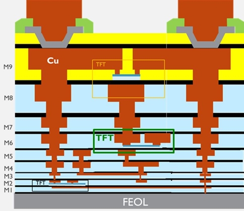
Integrating thin-film transistors (TFTs) at the level of intermediate interconnect layers is recognized as another opportunity of adding extra functionality to the BEOL. At this intermediate interconnect level, the via density is relatively low, creating empty space for small transistors such as TFTs. Here, they can be used for a variety of applications, including for example power management. First technologies with TFTs in the BEOL were mainly limited to Internet of Things applications.
Towards 3nm interconnects and beyond
The downscaling of device dimensions below the 5nm technology node is becoming increasingly challenging. This is mainly due to electrostatic and variability limitations in the front-end-of-line, and to routing congestion and a dramatic RC delay and wire congestion in the back-end-of-line. The RC delay results from a reduced cross-sectional area of the metal wires which drives up the resistance-capacitance product (RC) of the interconnect system. This, in turn, results in strongly increasing signal delay and power consumption. These problems started a few nodes ago and are becoming worse with each technology generation.
To continue interconnect scaling beyond the 5nm technology node, imec is exploring a variety of new process innovations, scaling boosters and materials. In particular, the toolbox for future interconnects includes the insertion of single-print extreme ultraviolet (EUV) lithography in dual-damascene integration flows, semi-damascene process flows in combination with air gaps, and scaling boosters such as Supervia structures for better routability (Figure 1). All these innovations call for new conductors, with better figure of merit than traditional Cu or Co. The toolbox is complemented with the integration of TFTs in the BEOL for a variety of additional functionalities. In the next sections, each of these novel interconnect building blocks will be discussed in more detail.

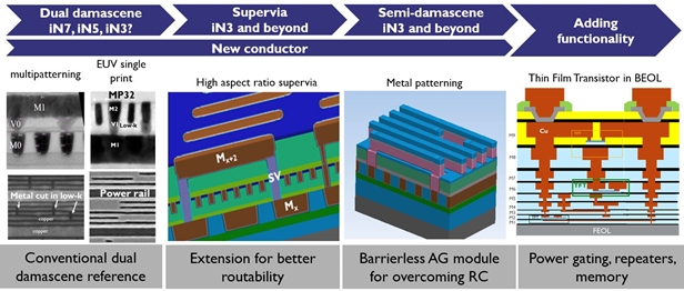
From dual damascene…
The semiconductor industry will extend the current dual-damascene technology as long as possible before moving to a new integration process. The key to extending dual damascene towards smaller metal pitches is the insertion of single-print EUV lithography for patterning the densest lines (M1 and M2) and vias (V1), which reduces process complexity. With respect to current immersion-based multi-patterning options, single print EUV will enable a cost-effective and significantly shorter process flow. True benefits of this approach are expected for printing metal pitches at least down to 30nm.
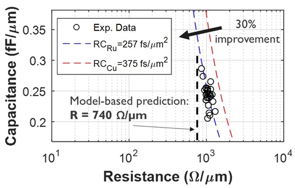
At IITC 2019, imec demonstrated a dual-damascene test vehicle relevant for manufacturing the 3nm logic technology node. The M1 layer was patterned with single-print EUV. To pattern the M2 21nm-pitch layer, a hybrid lithography approach was proposed, using 193nm immersion-based self-aligned quadrupole (SAQP) for printing the lines and trenches, and single print EUV for printing the block and via structures. The test vehicle implements a barrierless ruthenium (Ru) metallization scheme and an insulator with dielectric constant k=3.0. A 30% improvement in RC was obtained compared to previous generations, without impacting reliability (Figure 2).

Currently, the imec team is exploring the feasibility of realizing 16nm metal pitches. Realizing this aggressive pitch is challenged by variability and mechanical stability issues, and by an increasing complexity of the process flow – as multi-patterning options will be required.
…to semi damascene
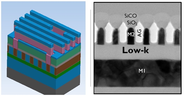
An interesting approach to extend damascene-based process flows towards 16nm metal pitches is the introduction of a semi-damascene module – which can exist in combination with traditional dual-damascene modules. The essential difference between dual damascene and semi damascene is the omission of the chemical mechanical polishing (CMP) step of metal – which is the final step in a dual-damascene process flow.
Semi-damascene processing starts with the patterning of a via opening and etching it into a dielectric film. The via is then filled with metal (e.g. Ru) and overfilled – meaning that the metal deposition continues until a layer of metal is formed over the dielectric. The metal is then masked and etched in order to form metal lines.
The true advantage of semi-damascene processing compared to single and dual damascene, is the ability to reduce variability and to form air gaps between the metal lines – as an alternative to conventional dielectrics such as SiO2. When combined with Ru as a conductor, no diffusion barrier between the dielectric and the conductor is required. This scheme limits the capacitance increase at high aspect ratios. Capacitance increase at higher aspect ratios is seen as a major obstacle for improving the RC of interconnects when using conventional dual-damascene flows. Higher aspect ratios are required for reducing the resistance and variability, but their positive effect is wiped out by the undesired capacitance increase. The use of semi-damascene modules with barrierless Ru air gaps can solve this problem.
Earlier, the imec team showed the feasibility of producing lines with metal patterning. Recently it was combined with EUV single print, resulting in uniform 30nm metal pitch lines (Figure 3).

Supervia structures for better routability
A next game changer in the interconnect landscape are Supervia structures, high-aspect ratio vias that connect, in their simplest form, an Mx layer with a Mx+2 layer. Supervias belong to the family of scaling boosters, introduced to reduce the number of tracks and, as such, the cell height of standard logic cells – as a way to further reduce chip area.
In its simplest form, the Supervia (Figure 4) provides a direct connect from an Mx to an Mx+2 metal layer by bypassing an intermediate Mx+1 layer in a self-aligned manner. Supervias and regular vias can co-exist in the same design, with the Supervia implemented on those locations where there would be a benefit for ‘jumping faster’.

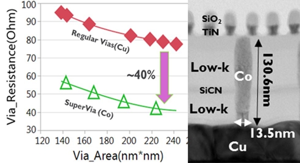
First use cases are SRAM constructs and buried power rail constructs – i.e., power rails buried in the chip’s front-end-of-line to help free up routing resources for the interconnects. At 2019 IITC, for example, imec demonstrated a Ru recess etch process with high resistance yield and low line resistivity – which is an essential step in the integration of buried power rails.
To extend Supervia structures beyond the 3nm node, imec has defined a roadmap containing a second (from Mx to Mx+3 and Mx+4) and a third (from Mx to Mx+5) generation of Supervias. This ultimate third generation, also called the ‘Ubervia’, is complex and still far from realization. But it would allow to immediately ‘jump’ to the wider metal lines, hence providing means for further reducing the RC metric.
Key enablers: Alternative conductors
Through the years, imec has been pioneering and pipelining the search for new metals to replace the more conventional Cu, tungsten (W) and Co in various interconnect applications. These alternative conductors will be key to realize the above-mentioned innovations, including the ‘next generation’ dual-damascene and semi-damascene modules, as well as the Supervia structures.
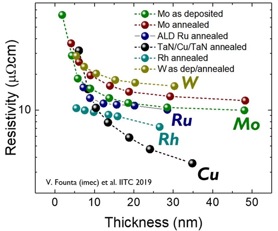
As a first step in the quest for alternative metals, a figure of merit (FOM) has been defined to allow for a ranking of the candidates. This FOM, defined as the product of the bulk resistivity times the mean free path of the carriers in the metal, is now widely recognized by the scientific community as a good starting point for the ranking – with Cu, W and Co as the reference materials. The metal with the lowest FOM is rhodium (Rh), followed by platinum (Pt), iridium (Ir), nickel (Ni), Ru, molybdenum (Mo) and chromium (Cr). The ranking however does not include metrics like cost, sensitivity to anneals or adhesion to the dielectric. Ir and Rh, for example, exhibit very poor adhesion to the dielectric, and especially Rh is very expensive – even more expensive than gold (Au). On the experimental side, for example, imec demonstrated that Mo is a very promising interconnect metal, especially as a potential replacement for W in scaled dimensions (Figure 5). The work on alternative metals has been presented at 2019 IITC.

The team also looked into binary and ternary compounds as alternatives for the conventional conductors. Especially the so-called MAX phases are doing better than pure elements – providing an opportunity for further research. MAX phases are layered structures composed of an early transition metal (M), an A-group element (A) and carbon or nitrogen (X).
Finally, the resistivity of metals such as Ru can also be lowered by capping the lines with graphene – which is known to be atomically thin, and have a high electrical and thermal conductivity, and high current carrying capacity. At IITC 2019, imec demonstrated lower electrical resistivity and higher thermal stability of fabricated graphene encapsulated Ru wires. These findings establish a possible route for hybrid carbon/metal interconnects.
Adding functionality to the BEOL
At the intermediate M6 to M8 interconnect level of advanced node chips, the via density is relatively low, creating empty space that can be used for implementing small transistors. Being small enough and temperature compatible, thin-film transistors can fulfill this task, thereby adding extra functionality to the BEOL (Figure 6).

Target applications are power management for both the server and mobile space, dual VT logic circuits, FPGAs (with large arrays of SRAMs), high-voltage I/O for voltage conversion, signal buffers for neuromorphic concepts. It can also find its way in DRAM memories or be used in selector applications for non-volatile memories.
The ultimate interconnect dream is to use them as repeaters, which occupy a big portion of the space in current designs. But for that both n- and p-type TFTs are required, the latter being not advanced enough for real implementation. Other challenges for BEOL implementation include the reliability, the maturity of the process technology on CMOS, and the cost – although at these ‘relaxed’ dimensions, simple single print immersion lithography can be used to make it more cost effective.
The imec team recently provided a hardware demonstration of functional indium-gallium-zinc-oxide (IGZO) TFTs on a 300mm wafer with low leakage, even at elevated temperature.
In summary
In this article, imec has presented several future scenarios that promise to extend interconnect scaling – which is challenged by the RC delay problem – towards the 3nm technology node and beyond. Area and cost scaling will be provided by enabling new options (e.g. the semi-damascene module), new scaling boosters (including the Supervia for better routability), new materials (such as alternative conductors and air gaps as dielectrics) and by adding functionality to the chips’ BEOL.
Editor’s Note: This article originally appeared in the November/December 2019 issue of Semiconductor Digest.