A molecule rotating on the surface of a crystal can function as a tunnel-gate of a transistor, as shown by researchers from the Paul-Drude-Institut für Festkörperelektronik (PDI) and the Freie Universität Berlin (FUB), Germany, the NTT Basic Research Laboratories (NTT-BRL), Japan, and the U.S. Naval Research Laboratory (NRL). Their complete findings are published in the 13 July 2015 issue of the journal Nature Physics. The team used a highly stable scanning tunneling microscope (STM) to create a transistor consisting of a single organic molecule and positively charged metal atoms, positioning them with the STM tip on the surface of an indium arsenide (InAs) crystal.
Dr. Stefan Fölsch, a physicist at the PDI who led the team, explained that “the molecule is only weakly bound to the InAs template. So, when we bring the STM tip very close to the molecule and apply a bias voltage to the tip-sample junction, single electrons can tunnel between template and tip by hopping via nearly unperturbed molecular orbitals, similar to the working principle of a quantum dot gated by an external electrode. In our case, the charged atoms nearby provide the electrostatic gate potential that regulates the electron flow and the charge state of the molecule.”
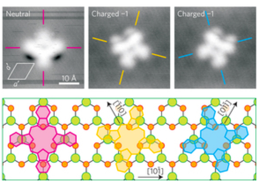
The Figure shows that the diameter of the device is ~4nm, so by conservative estimation we may take this as the half-pitch of closest-packed devices in IC manufacturing, which leads to pitch of 8nm. As a reminder, today’s “22nm- to 14nm-node” devices feature ~80nm transistor gate pitches (with “10nm node” planning to use ~65nm gate pitch, and “5nm node” ICs expected with ~36nm gate pitch). Thus, these new prototypes prove the concept that ICs with densities 100x more than today’s state-of-the-art chips could be made…if on-chip wires can somehow connect all of the needed circuitry together reliably and affordably.
—E.K.