Contributed by Dick James, Fellow Emeritus, TechInsights
At last year’s ISTFA conference, Chris Pawlowicz from TechInsights presented a paper “The Role of Cloud Computing in a Modern Reverse Engineering Workflow at the 5nm Node and Beyond” [1].
Integrated Circuit reverse engineering (RE) provides critical information to many players in the semiconductor business. Companies wanting to verify designs by taking off-the-shelf parts and recreating the electrical schematics of the original design (for competitive analysis, intellectual property infringement, security concerns, counterfeit parts, and failure analysis reasons), need their own RE capability or that of a company such as TechInsights.
RE of the circuitry in a silicon chip these days has plenty of challenges, especially as process nodes drop below the 5nm node. As technologies shrink, more circuitry is packed into a smaller area; to help reconstruct the original schematics, we need huge amounts of raw image data which has to be processed to extract the base level circuitry and then generate schematics and the subsequent heirarchies.
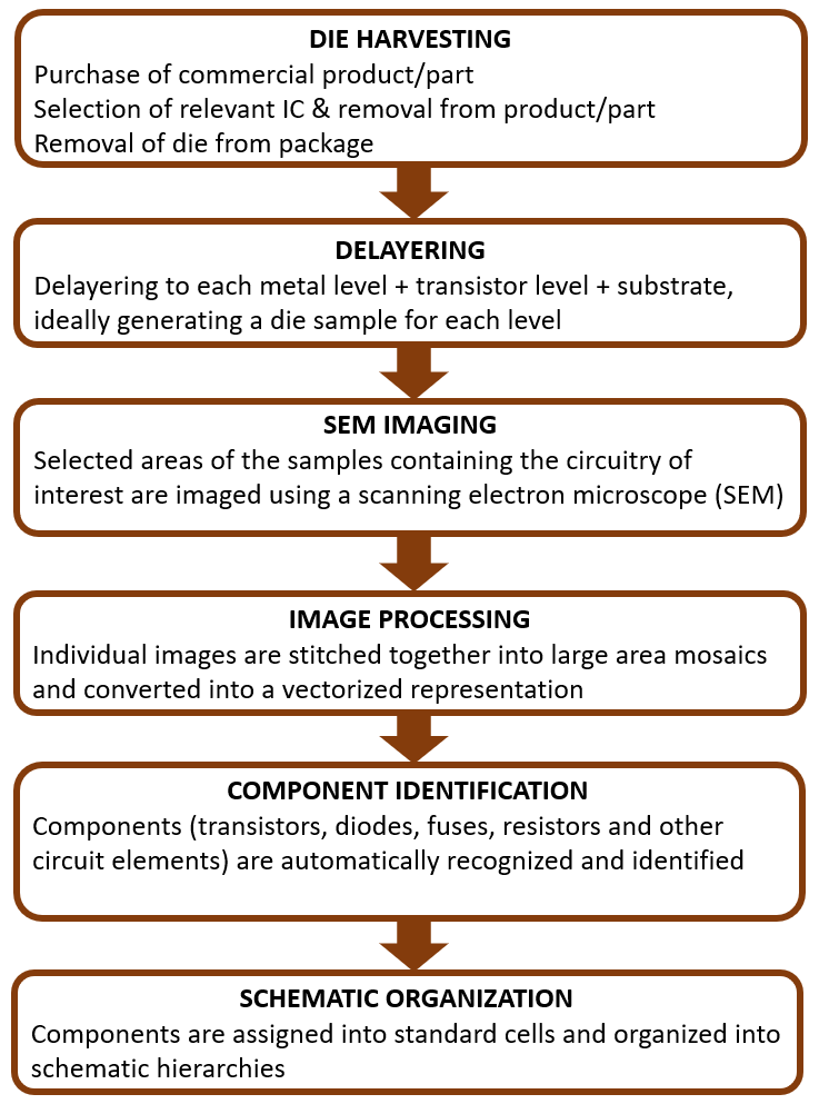
Reverse Engineering Workflow
For circuit extraction, the workflow is as shown below:

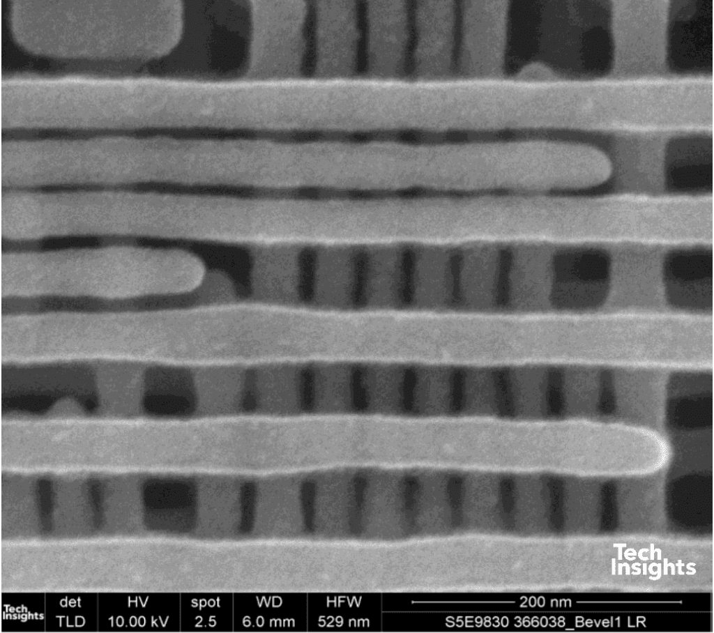
To achieve good feature discrimination in an image, each feature should be represented by at least 5 to 10 pixels. For the lower metal layers on a modern device, the metal pitch might be 36 nm with the space between the metal lines measuring 6 nm (see below, from a Samsung Exynos 990), so for accurate segmentation of the lower metal lines we would need to use 1-nm pixels at minimum.

To stitch adjacent images accurately we need registration precision better than 3 pixels (3nm), or metal wires could be joined incorrectly when creating the area mosaic. This mosaic then has to be converted to vectorized information (segmentation, i.e. conversion into polygons), so that the circuit interconnect can be traced and analyzed, usually with custom software.
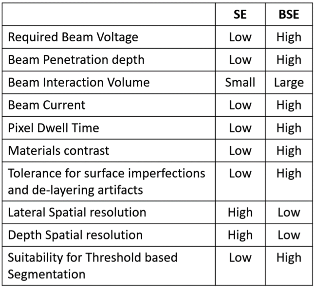
BSE images have higher material contrast and are often easier to segment, and because they aresub-surface they are less sensitive to artefacts caused by de-layering; and grey-scale value thresholding can often be used, which is computationally fast and inexpensive. We do not get something for nothing, however – they need much greater beam current, beam voltage, an longer pixel dwell times than for SE images, so slower imaging and lower resolution. The table below summarizes the differences:

And we can see the differences in these images:
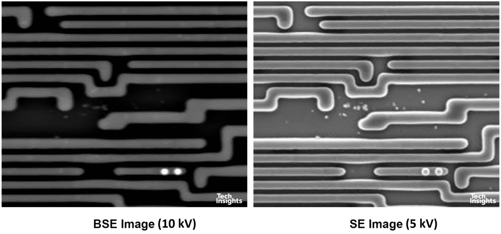

The left BSE image shows high materials contrast, whereas in the right image we can see more gradations in grey scale, as well as enhanced imaging of the sample-prep detritus between the metal interconnect lines.
Image Stitching
After imaging the image tiles have to be stitched together, making sure that we don’t lose any information between tiles. Unfortunately SEM stage accuracy is not good enough to align neighbouring images as generated, so the tiles have to be overlapped and then their exact position calculated during reconstruction.
Decades ago images were stitched manually, but now computer algorithms exist for automatically determining the best placement. These days there are tens of thousands of high resolution images for each layer, and the stitching must be accurate to within one or two pixels (i.e. one or two nm) on every seam.
Below we see a portion of two vertically adjacent tiles from overlapping images in their unstitched position. The red boxes show corresponding features in the two tiles, and to stitch them the bottom tile should be moved as shown by the red arrows. The translation varies from tile to tile due to inaccuracies in the stage positioning hardware.
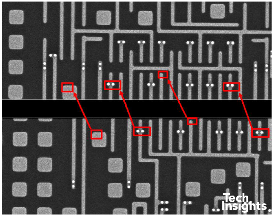

There can be problems in areas where many repeating similar features appear in the overlapping region (e.g. metal fill patterns or finger capacitor fingers), giving several possible matches. By comparing more than one edge we can often cure this, as shown below.
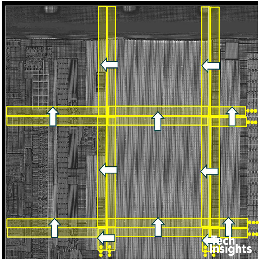

The upper-left tile is not bound to any other in this image, but all remaining tiles attach to their neighbours at either their top or right edges, and the tiles in the middle attach at both edges.
Any outliers can be found by expressing the translation coefficients as a system of linear equations in an overdetermined system, using optimization algorithms – after optimization, sorting by residual error can reveal the outliers.The stitching is improved by removing the outliers, rather than manually correcting them.
However, all of this needs a lot of compute power. Image correlation has become a bottleneck in the stitching process, as mosaics become larger and are captured more quickly. For example, for a mosaic of 240 tiles of 16384 x 16384 pixels/tile and a potential overlap of 60 x 16384 pixels, a simple four-threaded CPU takes ~15 minutes to complete correlation. As this is easily parallelizable, we can do it on a GPU, reducing the time to ~3.5 minutes; but programming is more complex and GPUs cost more.
Now we come to the cloud…
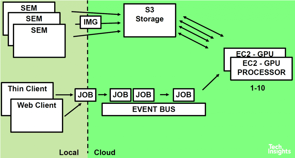
High-end workstations are getting more powerful every year, but they are expensive to purchase and operate. Now we are in a world where companies such as Amazon Web Services (AWS), Google, IBM, and others offer access to compute resources on a pay-per-use basis, with thousands of processors instantly available at per-second billing and virtually unlimited storage.
Parallelizable tasks such as image correlation are ideally suited to cloud computing, so we have adapted our image correlation algorithm to run on the AWS Lambda platform where each Lambda invocation performs the correlation for one tile seam. Using Lambda, we can run thousands of seam calculations in parallel with very little scaling overhead, and for the example above, runtime reduces to 2 minutes.
The TechInsights Circuit Studio design software used in the RE workflow now uses a hybrid approach – existing desktop workstations running local software to visualize and manipulate the data sets, connected to cloud computing for doing the processor-intensive calculations.
Image data is stored in S3 (Simple Storage Service), which allows massively parallel access, unlike hard drives, and repetitive tasks like stitching are split up into many discrete packets and placed on a job queue. Thousands of Lambda serverless auto-scaling compute processes are triggered automatically to grab the job packets, process them, and then shut down, keeping computation fast and costs low.
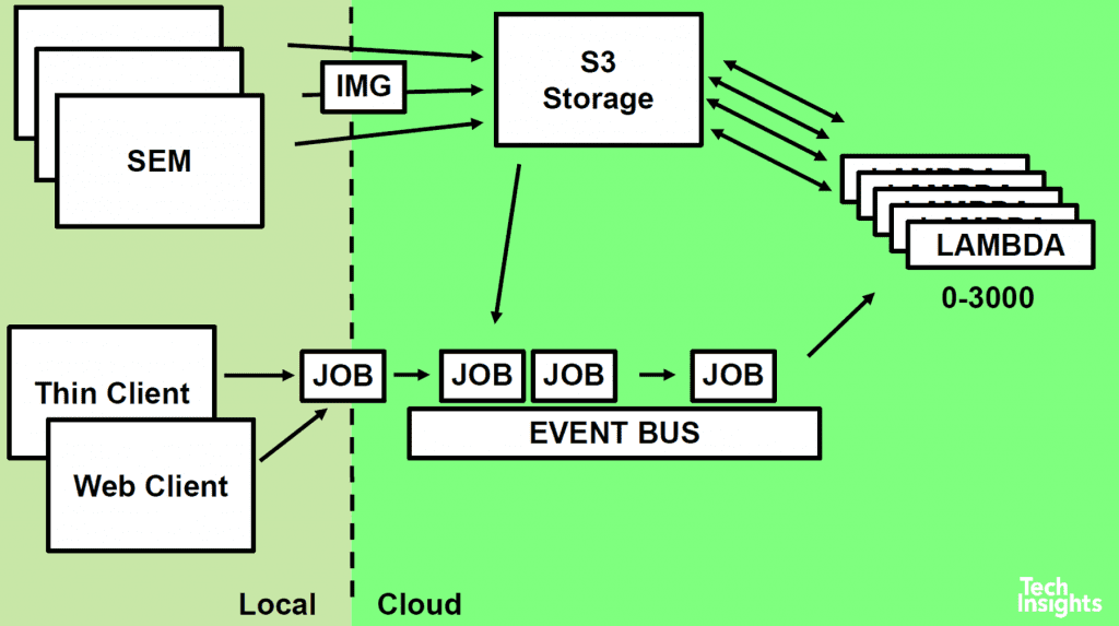

These calculations can be run in parallel with very little scaling overhead – scaling is automatic from 0 up to 3000 parallel instances currently, quickly scaling up or down to precisely match the number of jobs being run. The advantage offered by Lambda’s scalability gets better as mosaic size or overlap regions increases. For example, a mosaic of 567 tiles (each measuring 16384 per side) and an overlap region 16384 x 500 pixels has processing times of 17 minutes using Lambda, vs ~3 hours for GPU and 33 hours for a CPU.
Image Segmentation using Machine Learning
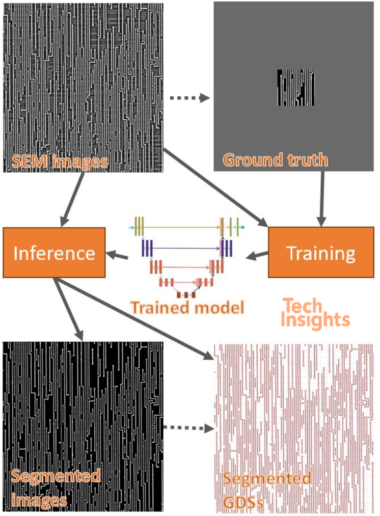
“Image segmentation” is the conversion of a grey-scale image into GDS-II type polygons:
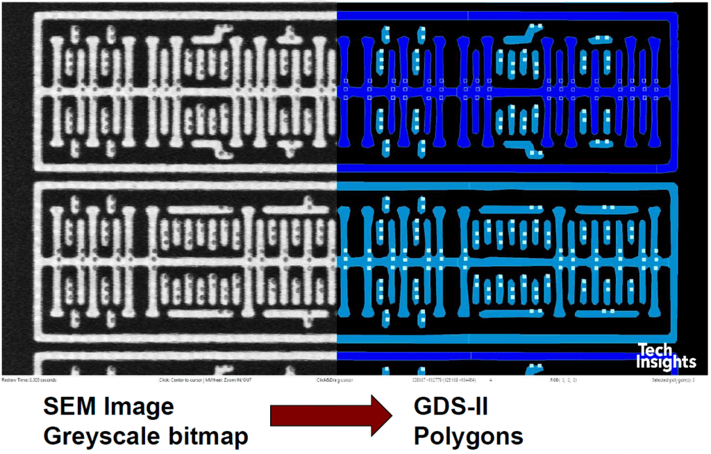

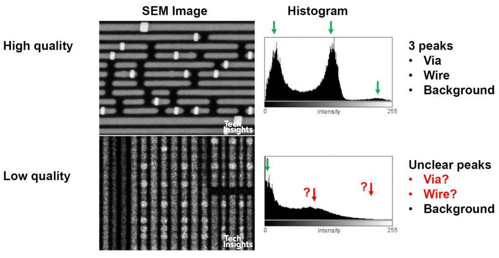
An 8-bit SEM greyscale image contains 256 shade variations. Ideally, the histogram of a “perfect” SEM image of a metal layer would show only three peaks: black for background (BG), grey for wires, and white for vias. Of course, that doesn’t happen in the real world, images are comprised of several shades of grey, which makes it difficult to use thresholding to define features, even with a blur filter.
To simplify the task, wires and vias are segmented in two different steps; two different image sets are acquired for the same region, one optimized to highlight vias, the other optimized to highlight metal wires.
The problem is, again, scalability: for a couple of images, a human operator can tweak the amount of blur and the threshold value for each image for optimal segmentation, but with thousands of images per grid this is impractical. Finding algorithms for automatic parameter selection of the threshold intensity gives variable and usually inaccurate results.

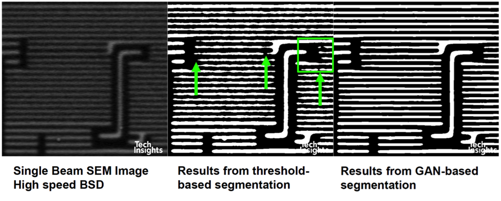

Vias are more difficult, since only a very small percentage of the pixels in an image belong to vias. We tried via segmentation using GAN, with better results than threshold, but not good enough, so we added a via classification CNN. After a strong blur filter, the via centers were detected using peak local intensity. For training, the imbalance of the data (i.e. vias vs the rest) was corrected by eliminating non-via patches and by data augmentation. This model gave results with recall and precision similar to the GAN model.
Independent of the method used, the results can be improved by model-based filters which remove small artifacts in the segmented image determined by size and/or shape. We are currently using a convolution-threshold filter which can remove small bridges and/or close small gaps, and also makes the results look smoother for the human operator.

GAN networks are particularly good for learning how to translate one image to another, in our case SEM to binary segmented images that can be converted to industry standard GDS-II format. These networks, on top of learning the mapping, also learn the loss function to allow this mapping to be trained; however, this may be overkill, since for binary segmentation the loss function can be selected and the complexity of training the GAN can be avoided. Because of that we are testing wires and via segmentation based on other network models such as: DCNAS, HRNet, DNL, etc. This is the typical workflow:

Now that we are in the era of ubiquitous cloud computing, we have fast and cost effective compute resources available, suitable for the compute-intensive processes in reverse engineering. In particular, we now use AWS Lambda serverless compute to speed up image registration by two orders of magnitude, and for segmentation, we use AWS EC2 Elastic Computer resources in combination with GAN Machine Learning to successfully segment SEM images of circuitry with greater accuracy than threshold based methods.
Isn’t technology wonderful!
Reference
- Pawlowicz et al., “The Role of Cloud Computing in a Modern Reverse Engineering Workflow at the 5nm Node and Beyond” ISTFA 2021, paper 26.2, pp. 561 – 564