Tony Key, Edwards Business Line Manager, Semiconductor Service , EMEA

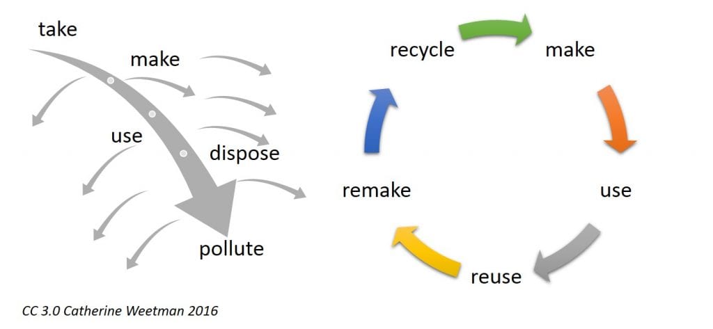
A circular economy is a model for economic activity that is restorative and regenerative by design. This contrasts with the conventional linear model – take, make and waste – that has dominated production design since that advent of the industrial revolution. To early industrialists the combination of non-animal power sources (steam) with seemingly unlimited material resources promised ever increasing production and decreasing cost. We know now that both energy and material are ultimately scarce and consumption of both carries unacceptable costs paid ultimately by the degradation of our shared environment. Circular economic design recognizes these costs and emphasizes reuse, sharing, repair, refurbishment, remanufacturing and recycling of materials through a circle of value, creating a closed system that reduces the consumption of resources and the creation of waste and pollution (Figure 1). Environmental costs are minimized, and economic benefits enhanced by more efficient use of resources.

Driven by our commitment to sustainable manufacturing and environmental stewardship, we at Edwards have worked hard to adopt the principles of circular economy across our design, production and support operations. For example, our dedicated EUV vacuum and abatement system (EUV Zenith) benefits from circular methods throughout its lifecycle. During manufacturing, the waste swarf from machining are collected and sent to the foundry to re-enter the supply chain as raw material. In use, most of the system’s components produce little waste and can be maintained on site. Utilities, like the water used to cool the vacuum pumps and quench the abatement, can be recycled. At end-of-life, when systems are removed from service, rather than being treated as waste and scrapped they are taken to a service technology center for remanufacturing. Many parts can be reused – the pump is sent back to the customer for continued use in the EUV lithography process. Metal components that do not meet specification are recycled to re-enter the manufacturing process as raw material.
The system was designed modularly to support the circular economy and enable prolonged product life. As the EUV process changes, it can be upgraded to meet new requirements with significant reuse of existing parts. Improvements made to increase availability or save energy are intentionally designed to require minimal new parts.
EUV lithography depends on a high, continuous flow of pure hydrogen and hydrogen consumption is an area of special concern. The hydrogen consumption of a single EUV lithography system is 20 times higher than for a typical epitaxial deposition chamber, and large, leading edge fabs will need multiple EUV systems. While hydrogen is abundant, being sourced from water or methane, such high-volume usage leads to concerns about energy consumption, carbon footprint, supply security and safety. A new sub-system that recovers and purifies hydrogen and returns up to 80% of it to the EUV lithography tool has been developed as an integral part of the vacuum and abatement system. The recycling system assures the purity and availability of hydrogen and reduces the overall carbon footprint of EUV lithography. Initial availability of this capability is scheduled for later this year or the first quarter of 2020.
Editor’s Note: This was originally published in the October 2019 issue of Semiconductor Digest.