By Dick James, Contributing Editor
At the International Electron Devices Meeting (IEDM) in San Francisco December 7-11, Geoffrey Yeap presented the talk “5nm CMOS Production Technology Platform Featuring Full-Fledged EUV and High-Mobility Channel FinFETs with Densest 0.021µm2 SRAM Cells for Mobile SoC and High-Performance Computing Applications”.
Even though I didn’t make it to the actual talk, we now have the proceedings paper, so we can give an update (in italics, apart from a few minor text edits).
Details of the 5-nm (N5) process have been slowly released over the last while, most recently at the Technology Symposium in April and the Open Innovation Platform Innovation Forum (OIP) last month, and also the Arm TechCon, all in Silicon Valley. Condensing the reported information from them, and in no particular order, we have:
- Aimed at both high-performance computing and mobile customers
- Risk production started in March 2019; high volume ramp in 2Q’20 at the recently completed Gigafab 18 in Tainan (phase 1 equipment installation completed in March’19)
- There will be a N5P (performance) version a year later, with a +7% performance boost at constant power, or ~15% power reduction at constant perf over N5
- Logic density is increased by 1.8X, SRAM scaling is 0.75, and analog scaling is ~0.85 vs 7-nm
- Iso-power speed gain is 15%, or 30% lower power at the same speed compared with 7-nm.
- EUV use was emphasised
- There will be a high-mobility channel (HMC) transistor
- Low-resistance contacts and vias; slightly relaxed metal pitch and wider vias.
- Transistor variants include an I/O transistor that can be either 1.5V or 1.2V, and an extreme LVT device 25% faster than the 7-nm equivalent.
- Via pillars and optimized metal in the HPC standard cells increase performance by 10%
- A 112Gbps SerDes is available.
- A super-high-density MIM-capacitor structure with 2X ff/µm2 and 2X insertion density, giving a 4% speed boost
- New low-K dielectric materials
- Metal Reactive Ion Etching (RIE), replacing Cu damascene for metal pitch < 30nm
- A graphene “cap” to reduce Cu interconnect resistivity
My thanks to Tom Dillinger at SemiWiki, Paul McLellan of Breakfast Bytes, and David Schor of WikiChip, for their diligent reportage.
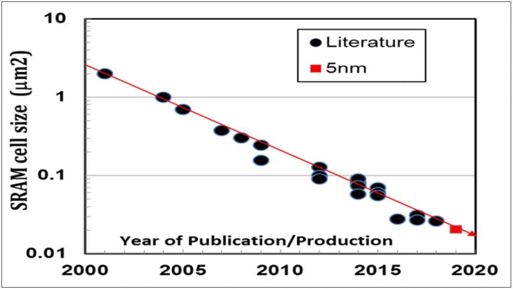
In the conference abstract details published by IEDM in their press kit, much of the above was reiterated. The logic density is a more detailed 1.84X, and the same 15% speed increase or 30% power drop over their 7-nm process are specified, as is EUV lithography (Fig. 2) and the high channel-mobility FinFET (Fig. 3). In addition, there are up to 7 Vts available (Fig.1). The company also says the high-density SRAM cell is the smallest ever reported, at 0.021µm2.
In a test circuit, a PAM4 SerDes transmitter demonstrated speeds of 130 Gb/s with 0.96pJ/bit energy efficiency. The technology passed qualification with high yield and mass production is expected in 1H 2020.
Fig. 1 below shows the 15% speed and density gains (left), and the seven Vt options.

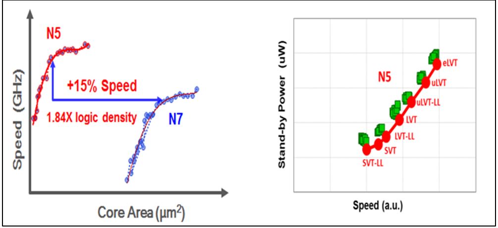
Fig. 2 illustrates the comparison of five immersion masks with a single EUV mask, in what looks like a standard cell routing layer, i.e. M1 or M2. With a tentative Mx pitch of 30 nm, that would need SAQP or LE3, plus a couple of cut masks, replaced with one EUV litho step. Using MxP of 30 nm to calibrate, this image gives us a track height of ~175 nm (~5.8 track cell), a linear scaling of ~0.73 compared with the 7-nm process. And we can see that the pattern is quite a bit sharper.

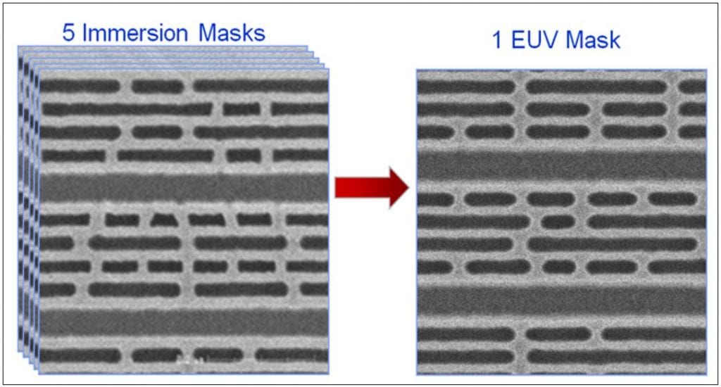
The paper claims more than ten EUV layers, replacing at least 4 times more immersion layers at cut, contact, via and metal line masking steps – 4x what they don’t say, but presumably N7+ (7FF+), the current EUV iteration. An EUV-based gate patterning process is also specifically mentioned. The 5-nm node is the first generation in TSMC in which the total mask count is reduced with the use of EUV (Fig 3).

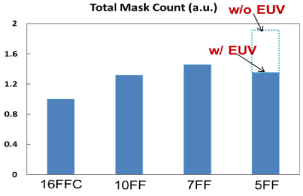

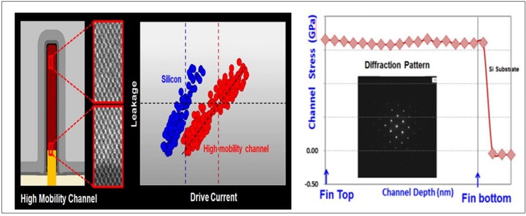
Fig. 4 (above) illustrates the improved drive current (+18%) in the high-mobility-channel transistor. There has been some comment that this might be a germanium channel (fin), but given the mis-match of the crystal lattices between Ge and Si, and the dislocations that would generate, it seems more likely that we have a PMOS SiGe channel similar to that used in the planar gate-first HKMG parts from the IBM consortium, containing up to 40% Ge.
The high-magnification TEM lattice images from a fin shown above indicate that the channel is the conventional <110> direction, though strangely the diffraction image on the right seems to be taken in the <100> direction.
No mention was made in the paper of the nature of the HMC channel, so I’ll stay with a SiGe channel. From what I can gather from reports of the Q&A session, no further information was given then either.
In the planar version the epi-SiGe was grown first, and then removed in the NMOS regions, in that case only 3 – 5 nm. If the active fin height is ~55 nm, and total fin height ~120 nm, that is a different challenge, but we now have very selective etches for SiGe vs Si as a result of all the recent work on nanosheet devices. A bigger problem to me is that if this method was used, the SiGe fins will be tens of nm higher than the Si fins, with added complexity in subsequent processing.
To keep the fins at the same level, I guess that we could go with an etch of the N- or P-areas, followed by epi of Si or SiGe plus CMP (or selective epi?), depending which area was etched; that doesn’t seem straightforward either. And I presume we’d have separate fin definition etches for Si and SiGe fins, which with quad patterning also sounds messy – maybe fin etch is now also EUV?
Given that a SiGe channel will have a different work-function from a pure Si channel, that raises the possibility (likelihood?) that we might have some PMOS devices with Si channels to add to the range of available PMOS Vts. The seven Vts announced is the most that we’ve seen; the Samsung 10-nm process analyzed by TechInsights seemed to have six, and Intel announced six in their 10-nm paper [1].

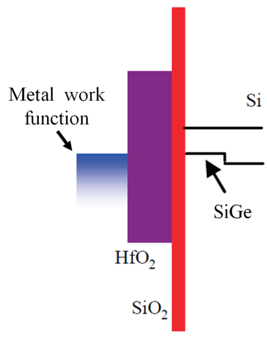
Fig. 6 below is simply a plot of published SRAM cell sizes, showing the 0.021µm2 SRAM is the smallest reported to date.


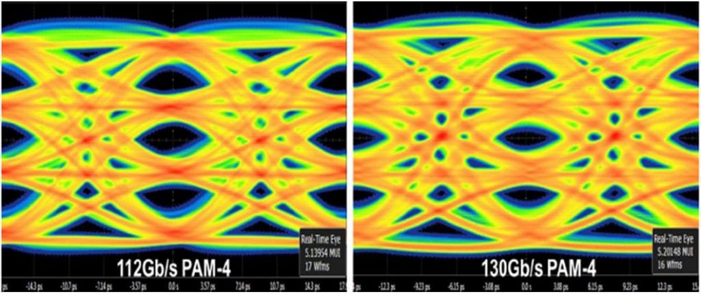
In Fig. 7 above we have eye diagrams for PAM4 SerDes transmitters built on a 5-nm test chip demonstrating the 112 Gb/s mentioned earlier and the 130 Gb/s detailed in the abstract.
When it comes to the back end, the Rc values for the tightest metal and via pitches are close to those for the 7N node:

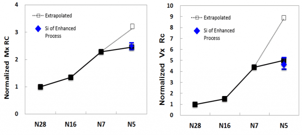
Apart from updated etch-stop and low-k layers, the earlier comments on the dry etching of copper metallization and graphene metal caps are not supported; it appears that the EUV patterning, an innovative scaled barrier/liner, and copper reflow have minimized the change in resistance numbers.
DTCO (Design-Technology Co-Optimization) features such as gate-contact-over-active and “unique diffusion termination” (some form of single diffusion break?) are incorporated with “smart scaling of major design rules”, to get 35%~40% reduction in chip size, although that is based on a mobile SoC design having 60% logic, 30% SRAM and 10% IO/analog content.
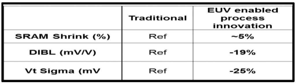
The EUV gate patterning also helps reduce SRAM cell size, DIBL, and Vt variation (table 1 below).

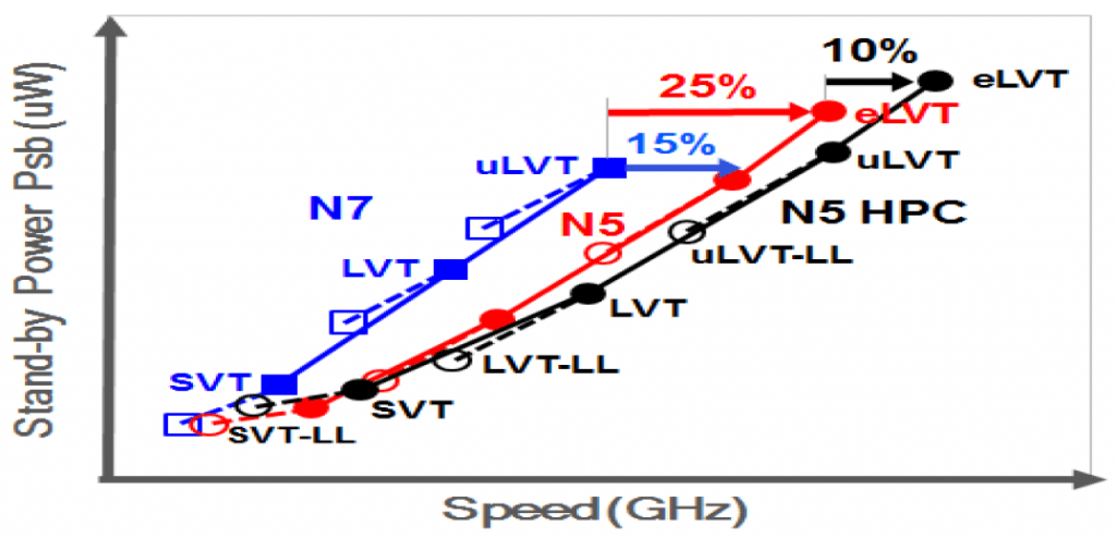
The extremely low Vt (eLVT) of the seven Vts shown above gives 25% peak speed over 7-nm, and a 3-fin standard cell allows an extra 10% performance boost for HPC (Fig. 8). I think that this will be the first time we have seen a 3-fin cell mentioned in a platform paper, apart from the 1-1-1 SRAM cell which is usually quoted as the smallest SRAM at a particular node (in this case 0.021µm2).

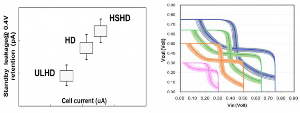
There are other SRAM cells available, as shown in Fig. 9; an ultra-low leakage (ULHD) cell can be used to improve better power efficiency, and a high-speed high-density (HSHD) SRAM gives the option of replacing as much HC SRAM as speed allows, giving area reduction of up to ~22%. Butterfly curves of the HD cell show operation down to 0.3 V.

A little more detail was given of the super-high-density MiM capacitor (Fig.10):

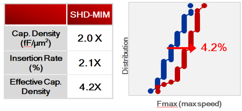
By minimizing transient drooping voltage, Fmax was improved by ~4.2%, and in a CPU test chip ~20mV Vmin reduction was attained.
You will have noticed that most of the information deals with performance and general technology advancements such as EUV and DTCO – no real numbers, and absolutely no pictures. While this was clearly an important paper, it is disappointing for us techno-nerds that no physical details of the process were given such as fin, CPP, and metal pitches.
To try and compensate for that, here are estimates from the estimable Scotten Jones (ICKnowledge, posted on SemiWiki) and David Schor (WikiChip Fuse) that they posted earlier this year:

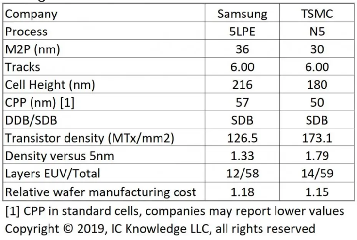

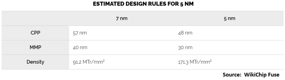
Slightly different CPP guesstimates at 50 and 48 nm, and minimum metal pitch at 30 nm, though Scotten has updated his MxP to 28 nm. Minimum fin pitch at N7 was 30 nm; if we take our estimated standard cell height of 175 nm from the EUV images, and make the broad assumption that it is a 2+2 (N fins + P fins) cell, then it is likely 7 fins tall. That also assumes gate-contact-over-active, which allows one fin spacing between NMOS and PMOS, and two shared fin spacings separating the cells above and below. 175/7 gives a 25-nm fin pitch, a 17% shrink, and do-able with SAQP or EUV.
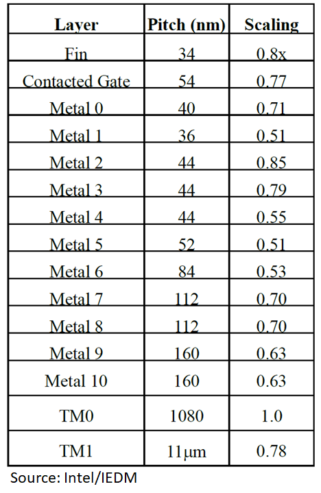
Just to emphasise the lack of detail in this paper, this is what Intel gave us in their 10-nm paper back at IEDM 2017:

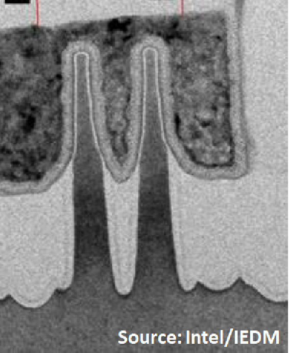
And a decent picture too:

I’m not the only commentator to have this complaint, other press colleagues and attendees have said the same thing, and with TSMC it’s not the first time. It puts the conference committee members in a dilemma, since this and similar papers are obviously high-profile and a draw for many people in the industry. But at some point the organisers have to push back and say “why bother?”. I can’t blame Geoffrey Yeap, it is clearly corporate policy, and in his previous role at Qualcomm he would likely have agreed with us.
One thing is clear, though – if the claims of high volume production in the first half of this year are accurate, we will likely see it in the new phones this autumn!
References:
- C. Auth et al., “A 10nm High Performance and Low-Power CMOS Technology Featuring 3rd Generation FinFET Transistors, Self-Aligned Quad Patterning, Contact over Active Gate and Cobalt Local Interconnects”, IEDM 2017, pp. 673 – 676
- H.R. Harris et al., Band-Engineered Low PMOS VT with High-K-Metal Gates Featured in a Dual Channel CMOS Integration Scheme, Symp. VLSI Technology 2007, pp 154-155