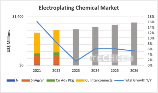

Stronger growth rebounds are expected in 2024 as demand for more devices for numerous applications (electric cars, more fast charging stations, more data storage, etc.) are expected to produce higher density and lower power devices. In addition, the US Chips Act and similar investments by Europe and China are expected to contribute towards market growth. Both these factors will drive more metal interconnect layers and more advanced packaging.
TECHCET’s Sr. Director, Dan Tracy, states, “Advanced Packaging requirements continue to be driven by increases in Wafer Level Packaging (WLP), and by consumption in the high-performance devices that utilize Redistribution Layers (RDL), interposers and Through Silicon Via (TSV) technologies.” Heterogenous integration, EMIB, Chiplets, and the power devices are expected to challenge the plating requirements in terms of quality of material being deposited.
Logic Gate All-Around (GAA) transitions node is planning to use backside power rails which appear to add at least four metal interconnect layers to the backside of the wafers.
TECHCET is following the introduction of Ruthenium or Molybdenum to possibly displace the Tantalum and Cobalt barrier layer at the GAA nodes. Ruthenium or Molybdenum (ALD or CVD, not plating) will possibly fill the interconnects and vias between M0 to M3 metal layers for Advanced Logic. Possible wafer backside connections to the backside power rail will add Copper plating to possibly match lost the loss of Copper plating at the M0-M3 layers.
For more details on the semiconductor Electroplating Chemicals market, supply-chain and growth trajectory, including supplier profiles on BASF, Dupont, Chang Chun Group, Ishihara Chemical/Unicon, and more, go to: https://techcet.com/product/metal-chemicals-for-fe-advanced-packaging/