NAOTO HORIGUCHI, director CMOS device technology, and Zsolt TOKEI, program director nano-interconnects, imec, Leuven Belgium
The manufacturing of leading-edge logic chips can be subdivided in three separate blocks: the front-end-of-line (FEOL), the middle-of-line (MOL) and the back-end-of-line (BEOL).
The FEOL covers the processing of the active parts of the chips, i.e. the transistors that reside on the bottom of the chip. The transistor serves as an electrical switch and uses three electrodes for its operation: a gate, a source and a drain. Electrical current in the conduction channel between source and drain can be switched ‘on’ and ‘off’, an operation that is controlled by the gate voltage.
The BEOL, the final stage of processing, refers to the interconnects that reside in the top part of the chip. Interconnects are complex wiring schemes that distribute clock and other signals, provide power and ground and transfer electrical signals from one transistor to another. The BEOL is organized in different metal layers, local (Mx), intermediate, semi-global and global wires. The total number of layers can be as many as 15, while the typical number of Mx layers ranges between 3 and 6. Each of these layers contains (unidirectional) metal lines – organized in regular tracks – and dielectric materials. They are interconnected vertically by means of via structures that are filled with metal.
The FEOL and the BEOL are tied together by the MOL. The MOL is typically made up of tiny metal structures that serve as contacts to the transistor’s source, drain and gate. These structures connect to the local interconnect layers of the BEOL. While cell size is scaling, the number of pins to connect to remains roughly the same – meaning that access to them is more challenging.
As device scaling continues to 3nm and below, the processing of each of these modules comes with many challenges – forcing chip makers to move to new device architectures in the FEOL, as well as to new materials and integration schemes in the BEOL and MOL.
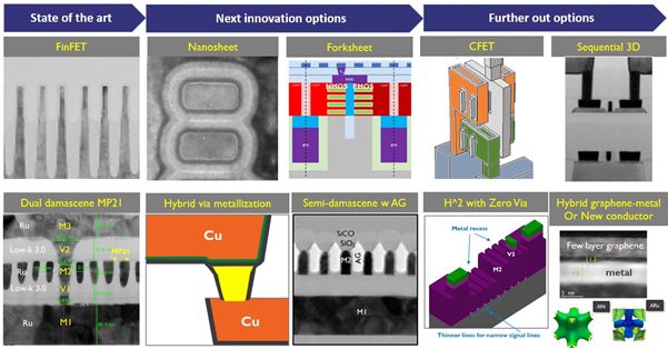
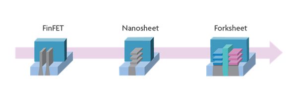
In this article, we present imec’s view on the scaling roadmap and dive into the various options (FIGURE 1). Starting from state-of-the-art mainstream FEOL, BEOL and MOL technologies, we gradually introduce new FEOL device architectures (i.e., gate-all-around (GAA) nanosheet, forksheet and complementary field effect transistor (CFET) devices). These architectures will immediately impact the local interconnect layers, calling for novel BEOL materials (such as ruthenium (Ru), molybdenum (Mo) and metal alloys) and novel integration schemes (i.e., hybrid metallization, semi-damascene and hybrid-height with zero via structures). Along this exciting journey, we also introduce structural scaling boosters (such as self-aligned gate contacts (SAGCs) and buried power rails (BPRs)) that help improving the connectivity of the MOL. These boosters will also help reducing the area at standard cell level, by allowing a reduction of the number of metal tracks at the level of local interconnects – referred to as track height scaling.

State-of-the-art mainstream technologies and their scaling bottleneck
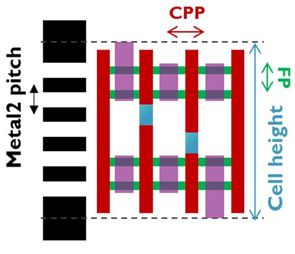
FinFETs at the FEOL: According to Moore’s Law, transistor dimensions scale down by 0.7x every two years. To maintain this scaling path, the industry moved from ‘good old’ planar MOSFET to the FinFET transistor architecture several years ago. In a FinFET, the channel between source and drain terminals is in the form of a fin, and the gate wraps around this 3D channel, providing control from 3 sides of the channel. This multi-gate structure could eliminate short-channel effects, which started to degrade the transistor’s performance at reduced gate length. In 2012, the first commercial 22nm FinFETs were introduced. Since then, the architectures were improved for enhanced performance and reduced area. For example, fin height was increased to obtain higher device drive currents at the same footprint. Today, the industry has 7nm chips in production with FinFETs ‘inside’. At the cell level of the most advanced nodes, standard cells with a track height of 6T feature down 2 fins per device, with contact pitches as small as 57nm. With 6T, we mean that 6 metal lines fit in the range of the cell height (FIGURE 2).

Cu- and Co-based dual-damascene at the BEOL: To keep up with area scaling in the front-end, BEOL dimensions have been reduced at an accelerated pace – leading to ever smaller metal pitches and reduced cross-sectional areas of the wires. Today, most critical local interconnects (being M1 and M2) have metal pitches as tight as 40nm. Cu-based dual damascene is the workhorse process flow for making the interconnects. A dual-damascene flow starts with the deposition of a low-k dielectric material on a structure. These low-k films are designed to reduce the capacitance and the delay in the chips. In next steps, vias and trenches are formed. Recently all leading logic manufacturers have announced the use of EUV lithography in their technology in order to remain cost effective at tight pitches. After patterning, a metallic barrier layer is added to prevent Cu atoms from migrating into the low-k materials. After coating the barrier layers by a liner and Cu seed, the structure is electroplated by Cu and then a chemical mechanical polishing (CMP) step is applied to complete the dual damascene module.
Routing congestion and a dramatic RC delay (resulting from an increased resistance-capacitance (RC) product) have become important bottlenecks for further interconnect scaling, driving the need for introducing new materials and integration schemes in the BEOL. Recently, industry has embraced Co as an alternative metal at the local level and some use airgaps at the intermediate layers as an alternative low-k dielectric material.
Contact resistance reduction and improved connectivity in the MOL: Connection between the FEOL and BEOL is provided by the MOL. For a long time, this MOL was organized as a single layer contact, but nowadays it is expanding into several layers, including for example the Mint and Vint layers. These layers carry the electrical signals from the transistor’s source, drain and gate to the local interconnects, and vice versa.
At the transistor side, the source/drain contact resistance has become an important concern for the chip industry. With shrinking transistor dimensions, the area available for making the contacts has decreased accordingly. This has caused a dramatic increase of the source/drain contact resistance – which is proportional to this contact area. Through the years, imec has developed improved source/drain contact schemes to mitigate the parasitic resistance – mainly by increasing the doping level at the semiconductor side, and by optimizing the interface quality between the metal (typically, a transition-metal silicide) and the semiconductor.
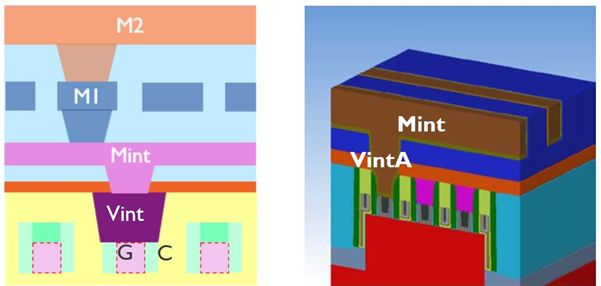
To further improve the connectivity in the MOL, structural scaling boosters have been introduced. One example is the self-aligned gate contact, which allows to place the gate contact directly on top of the active device (FIGURE 3). This has enabled a more flexible gate access and a reduction of the overall contact area. Industry has adopted this technique in today’s chip designs as to further improve routability.

Next innovation options for FEOL, BEOL and MOL
FEOL: vertically stacked nanosheet device and its extension to forksheet: As scaling is pushed beyond 5nm, the FinFET is expected to run out of steam. At reduced gate length, this device fails to provide enough electrostatic control of the channel. On top of that, the evolution to lower (5T) track height standard cells requires a transition to single-fin devices, which cannot provide enough drive current – even if fin height is further increased.
Here, vertically stacked gate-all-around (GAA) nanosheet transistors enter the scene. They can be considered a natural evolution of the FinFET device. Just imagine placing a FinFET on its side, and dividing it into separate horizontal sheets, which make up the channel. As the gate now fully wraps around and in between the channels, superior channel control is obtained compared to the FinFET. At the same time, the more optimal distribution of the channel cross-section in the 3D volume optimizes the effective drive per footprint.
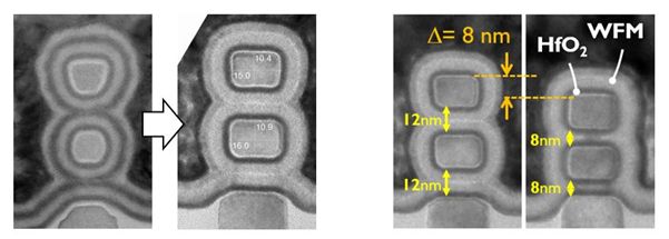
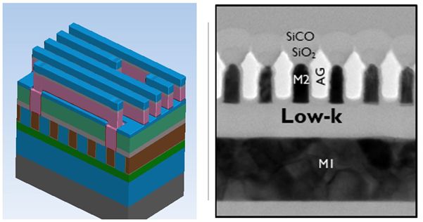
Imec has been working on this architecture since 2015, which has resulted in an optimization of the most critical process steps. The process flow for making vertically stacked GAA nanosheet transistors starts with an epitaxial deposition of multiple Si/SiGe layers, and the formation and filling of a shallow trench isolation (STI) module. In a later step, the SiGe layers are selectively removed, releasing the Si nanosheet structures. Around and in between these Si nanosheet layers, a gate stack is formed in a dual work function replacement metal gate (RMG) flow. Besides enabling optimized process steps, the imec team has developed processes to reduce the separation between the vertical nanosheets below 10nm (FIGURE 4). This way, the parasitic capacitance could be substantially reduced. Today, some of the chipmakers are preparing to move towards these devices for producing their next-generation chips.

To extend the scalability of the nanosheet device towards the 2nm node and beyond, imec has recently proposed an alternative architecture, called the forksheet device (FIGURE 5). In this architecture, the sheets are controlled by a forked gate structure, realized by introducing a dielectric wall in between p- and nMOS devices before gate patterning. This wall physically isolates the p-gate trench from the n-gate trench allowing a much tighter n-to-p spacing than what was possible with FinFET or nanosheet devices. Based on simulations, imec expects this forksheet to have superior area and performance scalability (allowing track heights to be shrinked from 5T to 4.3T), and lower parasitic capacitance. When implemented in an SRAM design, a reduced cell area can be expected.

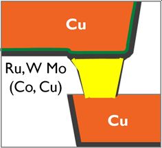
BEOL: hybrid metallization and semi-damascene: To keep pace with the area reduction achieved in the FEOL, metal pitches of the most critical local interconnect layers (M1 and M2) eventually will become as tight as 21nm. The vias in between these layers now have critical dimensions as small as 12-14nm. In a conventional Cu dual-damascene integration scheme, a barrier and liner layer are deposited within the trench and via structure before the actual Cu metallization. But at these tight dimensions, the liner/barrier is taking up too much room, leaving little room for the Cu fill. This negatively impacts the via resistance and variability, which now have become a limiter. Furthermore, due to the high current density requirements, electromigration reliability is challenged. One of the options to overcome this challenge is hybrid metallization, where an alternative via metal (such as Ru, W or Mo) connects in a barrierless fashion to the bottom of the Cu line (FIGURE 6). This construct allows for a thinner (2nm) Cu line barrier, while maintaining electromigration reliability and at the same time lowering the resistance of the via. While such a scheme can be attractive from resistance point of view, it is key that it is also reliable – which is an area of active research in order to come to solutions.

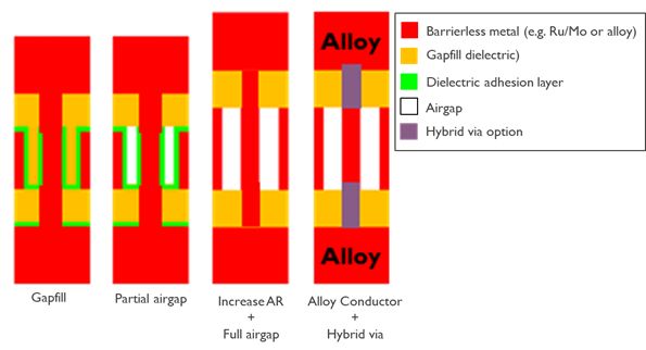
For metal pitches below 21nm, imec proposes semi-damascene as an interesting option (FIGURE 7). Key for semi-damascene that it allows for interconnect height increase, while keeping capacitance under control, so overall promising RC benefit.

From process technology point of view, it uses patternable alternative metals and eventually airgaps. The essential difference between dual damascene and semi damascene is the omission of the chemical mechanical polishing (CMP) step of metal – which is the final step in a dual-damascene process flow. In semi-damascene processing, the via is patterned in single damascene fashion, then it is filled with metal and overfilled – meaning that the metal deposition continues until a layer of metal (i.e., a barrier-less metal such as Ru or Mo) is formed over the dielectric. The metal is then masked and etched in order to form metal lines. This way, lines with higher aspect ratios – and hence, lower resistance – can be formed as opposed to dual-damascene processing. After metal patterning, the gaps between the lines can be filled by a dielectric or can be used to form partial airgaps at the local layers.
For a second generation, full airgaps are envisioned and, at a much later stage, ordered metal alloys could be used as a conductor. This sequence leads to gradual improvements from generation to generation. The use of airgaps limits the capacitance increase that would result from implementing higher aspect ratio lines. This semi-damascene integration scheme, envisioned for the most critical metal layers M1 and M2, can be combined with conventional dual-damascene or hybrid metallization schemes for the less critical interconnect layers above (FIGURE 8).

MOL: connectivity revolution, supported by scaling boosters: In the MOL, we already saw the introduction of structural scaling boosters to improve routability. This connectivity (r)evolution will continue, allowing other implementations of the MOL layers – depending on the connection needs between the devices and the interconnects. The forksheet device architecture, for example, allows a more flexible gate connection and gate cut – resulting in increased routing flexibility.
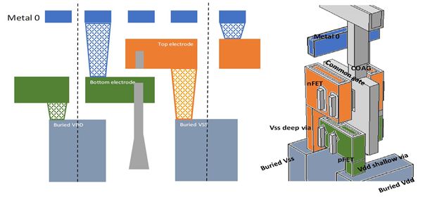
Another emerging booster is the buried power rail (BPR). Power rails are part of the power delivery network and are traditionally implemented in the chip’s BEOL (i.e., the Mint and M1 layers). BPRs on the contrary are buried in the chip’s FEOL to help freeing up routing resources for the interconnects. This challenging construct directly impacts both the FEOL and BEOL fabrication. At VLSI 2020, imec presented a tungsten (W) buried power rail (BPR) integration scheme in a FinFET CMOS test vehicle, which did not adversely impact the CMOS characteristics. Complementary assessment studies also showed the advantages at system level of implementing BPRs as a scaling booster in logic and SRAM designs.
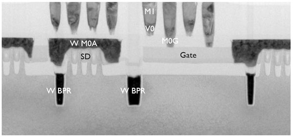
This integration scheme can be extended with so-called VBPRs – in which the via to the BPR now stitches with the MOL layer (M0A line). At VLSI 2020, the imec team showed a tungsten based BPR which was interfaced with a Ru via (the VBPR) to contact with Ru M0A lines (FIGURE 9). For this construct, excellent resistance and electromigration results were obtained.

In addition, innovations are needed that allow to further decrease the source/drain contact resistance. Imec has proposed improved contact schemes, including wrap-around contacts (enabled by atomic layer deposition of the metal) as a replacement for diamond epi contacts. This re-enlarges the contact area and as such decreases the contact resistance.
Further out options: continuing the journey towards 1nm nodes
CFET in the FEOL: the road towards 3T logic standard cells: Beyond 5T, a further reduction of the cell height is now mainly limited by routability issues – which should be evaluated at the logic block level. Optimizing routability brings us to the CFET – pushing the horizon for Moore’s Law further out. The concept of CFET consists in ‘folding’ the nFET on top of the pFET (either fin-on-fin or sheet-on-sheet) – as such fully exploiting the possibilities of device scaling in 3D (FIGURE 10). The strongest advantage of this architecture is area scaling, eventually enabling 3T logic standard cells and SRAM cells with significantly smaller layout area.

At VLSI 2020, imec showed a first experimental proof-of-concept of the CFET device, which was fabricated in a monolithic process flow. The team managed to overcome the critical process challenges of this complex process scheme, where CFETs are processed from bottom to top starting from a bulk substrate. Today, sequential CFET is being explored as an alternative, less complex integration flow. In sequential CFETs, processing of the bottom tier device (e.g. pFET) is followed by wafer bonding to form the top tier device (e.g. nFET) channel, and the top tier device is further processed. Sequential CFET gives a more flexible choice of the channel materials to be used in the top tier device.
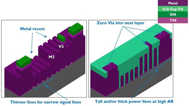
BEOL: ‘hybrid height with zero via’, and the search for alternative conductors: Resistance and capacitance of the metal lines and vias remain the most critical parameters of the BEOL. One way to cope with this issue is an alternative metallization construct – referred to as ‘hybrid height with zero via’. This scheme allows to flexibly exchange resistance for capacitance, depending on the application need of the metal line.
The idea is to split each metal layer into three separate sub-layers: a center line, and a possible extension above or below. For each metal layer, we now end up with four possible scenarios (only center line; center line + extension down; center line + extension up; center line + extensions up and down). This allows us to tune the height and aspect ratio of the metal lines within the same footprint. For example, if the line needs to serve as a power rail which is very resistance sensitive, lines with a high aspect ratio (and hence, low resistance) can be formed. If the line needs to carry a signal, only the center line is used as to keep the capacitance low. This construct not only provides flexibility to exchange resistance for capacitance, it is also expected to improve the overall energy and speed.
From processing point of view, the different heights are realized by metal recess etching steps. By recessing all the way to the end, the line can be used as a vertical via connection – omitting the need for a classical via construct. Imec is addressing the various challenges that come along with the processing of the ‘hybrid height with zero via’ construct shown in FIGURE 11.

In addition, lowering the standard cell area to 3 to 4 tracks will require conductors with extremely low resistance. Imec explores a myriad of new conductor materials that promise to have a better figure of merit than Ru and Mo. This figure of merit is defined as the product of the bulk resistivity times the mean free path of the carriers in the metal. Of interest are ordered binary intermetallic compounds with low resistivity at very scaled dimensions. Examples are Ru and Al based compounds, such as AlNi or RuV3, although not the only candidates. Ab initio calculations have shown promising properties for a variety of metals for future interconnect applications. The search for the next new conductor is not easy, but what is encouraging is that several R&D groups around the world have embraced the idea and are looking for candidates.
On the longer term, a hybrid graphene/metal conductor is an interesting alternative as well. Graphene is known to be atomically thin and has a high electrical and thermal conductivity. However, the material does not hold enough charge carriers to be useful as a local interconnect. But, there are ways to modulate the conductivity. One way is to use a hybrid metal/graphene scheme in which the metal (e.g. Cu, Ru, Mo, etc.) is encapsulated by graphene. Imec earlier demonstrated low electrical resistivity and high thermal stability with such a hybrid metal/graphene option.
MOL: A further innovation of the MOL layers will be needed to further relax the routing congestion and to cope with the demands of the newly proposed transistor architectures. In CFET, for example, novel solutions are needed for contacting the gate – that will now be common to the n- and pFET devices. In addition, high-aspect ratio vias will interconnect the various building blocks – that have now expanded into the third dimension. However, the dominant parasitic resistance of these deep vias needs to be reduced. This can be achieved by introducing advanced MOL contacts using e.g. ruthenium.
In summary
As scaling continues beyond 5nm, chip makers may gradually move away from mainstream technologies such as FinFETs (in the FEOL), Cu dual damascene (in the BEOL) and traditional contact schemes (in the MOL). In this article, we have presented next and further out innovation options for FEOL, BEOL and MOL – providing a possible path towards the 1nm technology node.
About the authors


Zsolt Tokei is program director nano-interconnects at imec. He joined imec in 1999 and since then held various technical positions in the organization. First as a process engineer and researcher in the field of copper low-k interconnects, then he headed the metal section. Later he became principal scientist, and program director nano-interconnects. He earned a M.S. (1994) in physics from the University Kossuth in Debrecen, Hungary. In the framework of a co-directed thesis between the Hungarian University Kossuth and the French University Aix Marseille-III, he obtained his PhD (1997) in physics and materials science. In 1998 he started working at the Max-Planck Institute of Düsseldorf, Germany, as a post-doctorate researcher. Joining imec, he continued working on a range of interconnect issues including scaling, metallization, electrical characterization, module integration, reliability and system aspects.
About Naoto Horiguchi


Naoto Horiguchi is a director of the logic CMOS scaling program in imec, Leuven, Belgium. He started his carrier in semiconductor device R&D in Fujitsu Laboratories Ltd. in 1992. In 1992-1999, he was engaged in device development by using semiconductor nanostructures in Fujitsu laboratories Ltd. and University of California, Santa Barbara. In 2000 to 2006, he was engaged in 90-45nm CMOS technology development in Fujitsu Ltd. as a lead integration engineer. From 2006, he is with imec, Leuven, Belgium, where he is engaged in advanced CMOS device R&D together with worldwide industrial partners, universities and research institutes. His current focus is CMOS device scaling down to 2nm technology node and beyond.