Contributed by Dick James, Fellow Emeritus, TechInsights
Last November AMD held their AMD Accelerated Data Center Premiere, Intel had their Innovation Days, and Stephen Shankland of CNET visited Intel’s fabs 42 and CH-4 in Chandler.
AMD
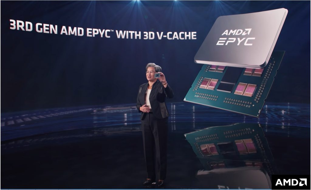
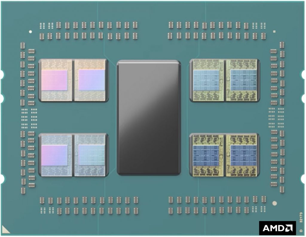
At the premiere, AMD chief Lisa Su introduced the new Milan-X, the third gen AMD EPYC processor with 3D V-cache.

It has eight Zen 3 CCDs with 6 x 6 mm 64 MB SRAMs hybrid bonded to each CCD, so essentially the same SRAM die as we reported earlier this year after Computex.
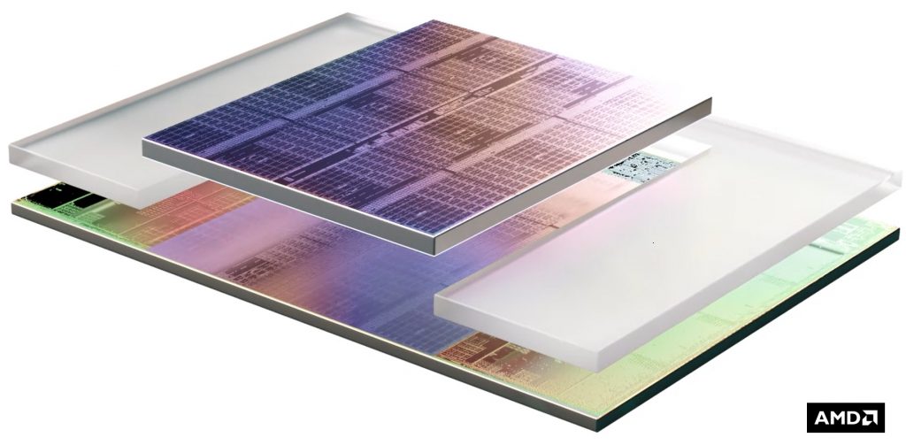


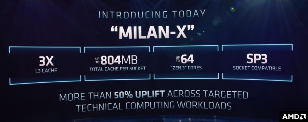
AMD is clearly satisfied with TSMC’s SOIC hybrid-bonding technology now that they are launching this new high-profile product, with eight such dies per device.

Later in the keynote, AMD SVP/GM of the Data Center and Embedded Solutions Group Forrest Norrod discussed the new AMD Instinct MI200 series of accelerators. They contain two CDNA2 GPU dies, for a total of 58 billion transistors in a 6-nm technology, with up to eights stacks of HBM2E memory, making it the world’s first GPU available with 128 GB of HBM2E. This caught our 3D-packaging attention since they use an “Elevated Fanout Bridge”.
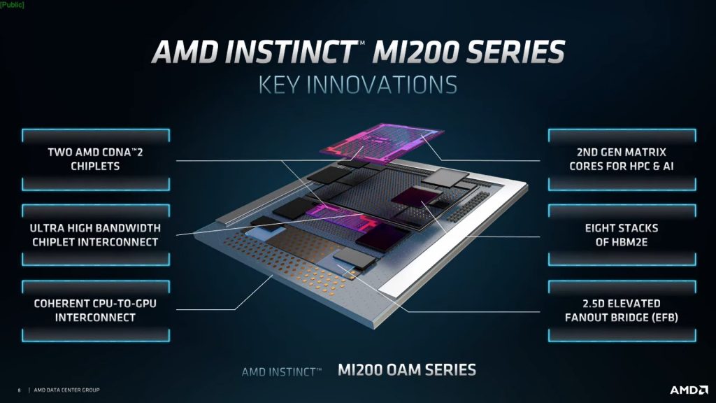

This is in essence a connector die like Intel’s EMIB and TSMC’s InFO-LSI, but on top of the substrate PCB instead of embedded into it.
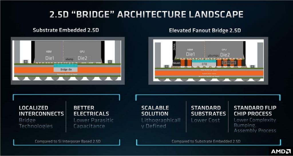

AMD has a patent on this type of structure (US 10,867,978).

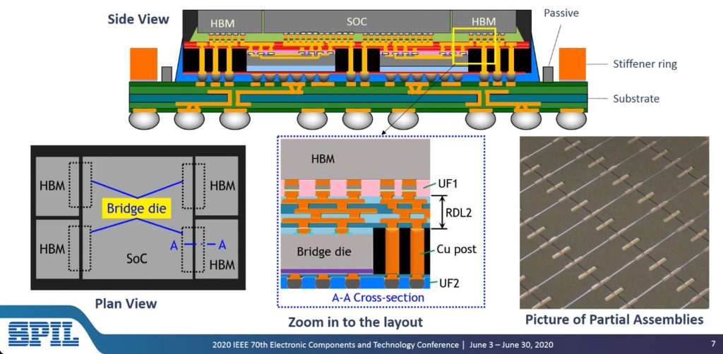
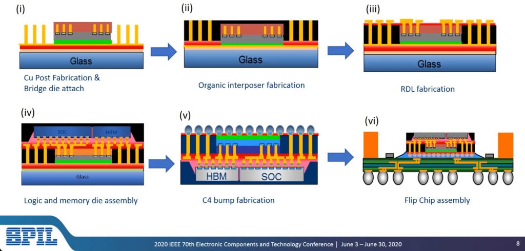
Which inclines me to think that AMD will be using an OSAT for this technology rather than TSMC. As it happens, SPIL (Siliconware Precision Industries Co., Ltd) has a similar technology that they announced at ECTC 2020 [1], labelled “Fan-Out Embedded Bridge”.
Which uses a bridge-first sequence to put the assembly together:


At the SC21 conference a couple of weeks ago, AMD exhibited a HPE Cray EX235a node, which uses the AMD Instinct MI250X, and the sharp-eyed Patrick Kennedy of Serve The Home spotted it and posted the details, so we know that that Instincts are at least being sampled to OEMs.
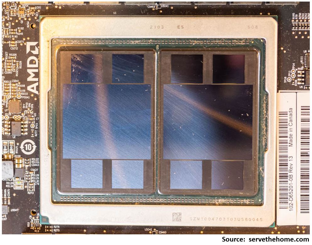

No sign of the EFBs, but presumably our view is obscured by the underfill.
Intel
There was actually not much mention of packaging at the Intel event, although they did discuss

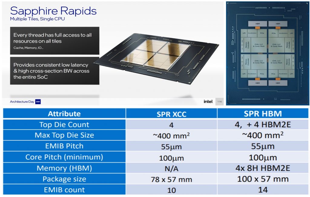
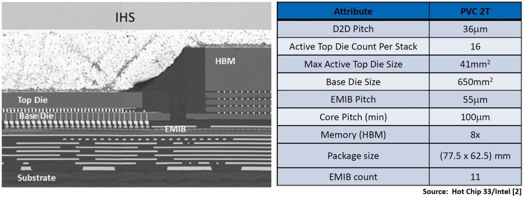
As we can see, the SPR dies are ~400 mm2, and there 10 EMIB dies connecting them, with another four for the four HBM stacks when they are used.
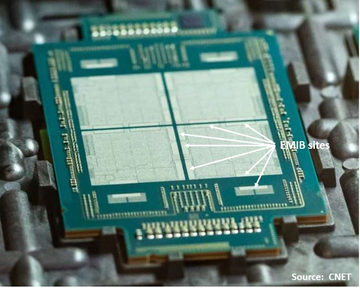
When Stephen Shankland visited Intel’s CH4 packaging fab, he snapped a picture of the SPR substrate, showing where the EMIB dies sit.


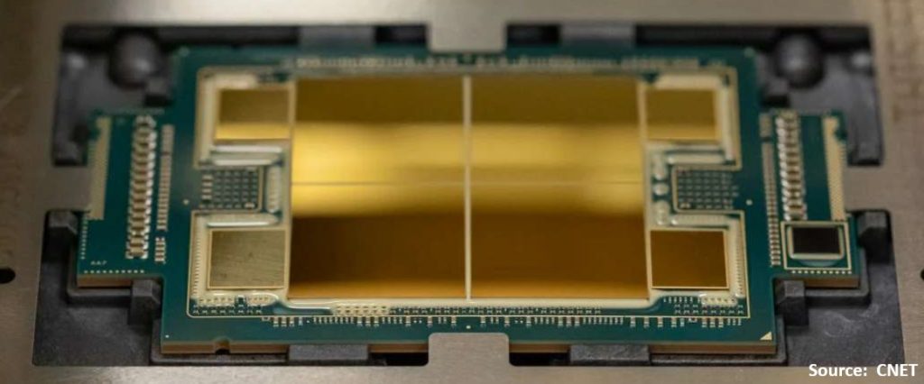
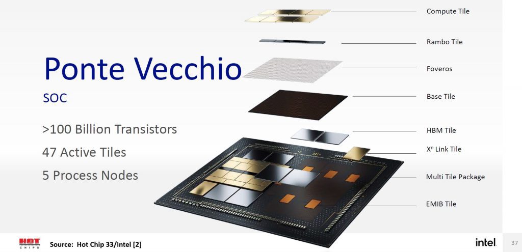
Intel has been promoting their Ponte Vecchio (PVC) high-end GPU for a while now, with its liberal use of Foveros die stacking and EMIB interconnect.


CNET also saw a slab of four assembled PVC parts:
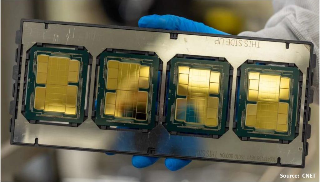

We see four dies there, so presumably one is a filler, since Meteor Lake consists of discrete compute, GPU, and low-power SoC tiles. While one or more tiles are from foundries, the compute tile is fabbed in the Intel 4 process (formerly 7-nm), and is functioning, according to Pat Gelsinger at the Q3 call:
“On Intel 4, we had taped out our compute tile for Meteor Lake and this quarter it came out of the fab and powered up within 30 minutes with outstanding performance, right where we expected it to be. All told, this is one of the best lead product start-ups we have seen in recent memory, which speaks to the health of the process.”
I think that we can clearly say that we are now in the chiplets era!
References
- Lin, et al., “Scalable Chiplet Package Using Fan-Out Embedded Bridge”, ECTC 2020, paper 1.3, pp. 14 – 18
- Mahajan, “Advanced Packaging Technologies for Heterogeneous Integration”, Hot Chips 33, 2021, tutorial