AJAY BARANWAL, Center for Deep Learning in Electronics Manufacturing (CDLe); NORIAKI NAKAYAMADA, NuFlare Technology; MIKAEL WAHLSTEN, Mycronic; and AKI FUJIMURA, D2S
Advanced photomasks are increasingly adopting non-orthogonal patterns and complex shapes, such as curvilinear mask patterns, due to the need for aggressive optical proximity correction (OPC) and inverse lithography technology (ILT) to produce leading-edge semiconductor devices with smaller feature sizes. Performing scanning electron microscopy (SEM) image analysis of these complex masks during the fabrication process at the mask shop is critical to identifying defects and other mask writing errors that can negatively impact yield. With sub-nanometer accuracy, SEM imaging is the only method that provides sufficient resolution to perform final mask analysis, particularly for EUV masks with the smallest feature sizes.
The use of deep learning (DL) in mask SEM image analysis is an attractive alternative to tedious and error-prone processes performed manually by operators and engineers. DL applications are programmed by data, instead of by writing a task-specific algorithmic code. To build a meaningful, high-performance DL model, it is necessary to collect a large volume of different types of SEM image data. Hundreds of thousands or even millions of SEM images may be needed to build up a sufficiently accurate DL model. Obtaining this extremely high volume of SEM images is laborious and impractical, particularly since real SEM images containing a large variety of potential defects are hard to obtain. This is because actual mask yield problems in the mask shop are intentionally rare (albeit costly) occurrences.

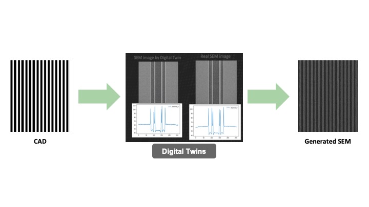
Digital twins that can produce images from CAD data that mimic real mask SEM images provide a way to synthesize ample data for training DL models. However, the question remains whether the images generated by digital twins are of sufficient quality to train a DL network that then performs well with real SEM images. In this article, we detail our use of mask SEM digital twins to create SEM images to serve as training data for two kinds of mask analysis: CAD to SEM image alignment and variable-shaped beam (VSB) mask-writer defect classification. In each case, we evaluated the accuracy of the digital-twin-trained DL network on test cases using real SEM images.
Read the full article in the April/May issue of Semiconductor Digest.